
| brainstorm | Posted: 17 Jul 2020, 02:16 PM |
|---|---|
 @braincode Member Posts: 9 Joined: 16-July 20 |
This is a continuation on my ramblings from this thread comment, I didn't want to steal the OP's thunder on the GamePad: https://mitxela.com/forum/topic/mocute-051-bluetooth-gamepad-bk3231-change-hid-profile-from-keyboard-gamepad#1594910340 After squinting at the BK3231 datasheet (asserting PPROG pin high to be able to talk with the SPI pins): https://pdfhost.io/v/3r1I3HggE_BK3231_Bluetooth_HID_SoCpdf.pdf And with this Arduino sketch connected with the mess of wires:
I'm getting the following readings on the oscillosope: 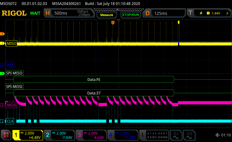 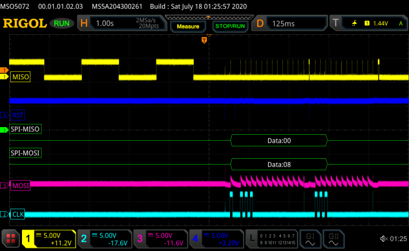 Would anybody want to join me on the quest to dump the internal flash? ;) Last edit by brainstorm at 19 Jul 2020, 12:31 PM ------------- |
| [top] | |
| mit | Posted: 18 Jul 2020, 11:53 AM |
 yeah whatever Admin Posts: 687 Joined: 4-May 16 |
Nice work. I'm not sure I'll be able to help with this, but I'd be keen to hear more if you get any further. ------------- |
| [top] | |
| brainstorm | Posted: 19 Jul 2020, 01:13 PM |
|
@braincode Member Posts: 9 Joined: 16-July 20 |
Thanks Mitxela! Yes you can help a ton by peer reviewing my steps and thoughts! :) At the moment I'm a bit confused by the datasheet (I just reuploaded the PDF so that viewers are not faced with allaboutcircuits user/pass screen): https://pdfhost.io/v/3r1I3HggE_BK3231_Bluetooth_HID_SoCpdf.pdf At the memory organization section, there is this paragraph towards the end: === By setting PPROG-pin to 1, the internal FLASH program memory can be written with four GPIO as a SPI slave. To access the FLASH memory **with internal program**, please refer to MFC section for detail. === Which seems to imply that the MFC procedure does not apply for "non-internal programs", i.e communicating from outside as I'm doing? That would rule out the MFC steps outlined on the gamepad thread (see below for screenshot)? Then there's the SPI section of the datasheet. I guess that the right way to read some data from other memory regions via SPI would be sth like (pseudocode):
But after I configured the SPI parameters, I don't see any straightforward way to exfiltrate internal flash program memory by reading 0x2 SPI_DATA register on a loop. Which leaves me to perhaps focus on poking MFC instead via SPI on the described 7 steps from that section, even if the program is running outside the MCU?: 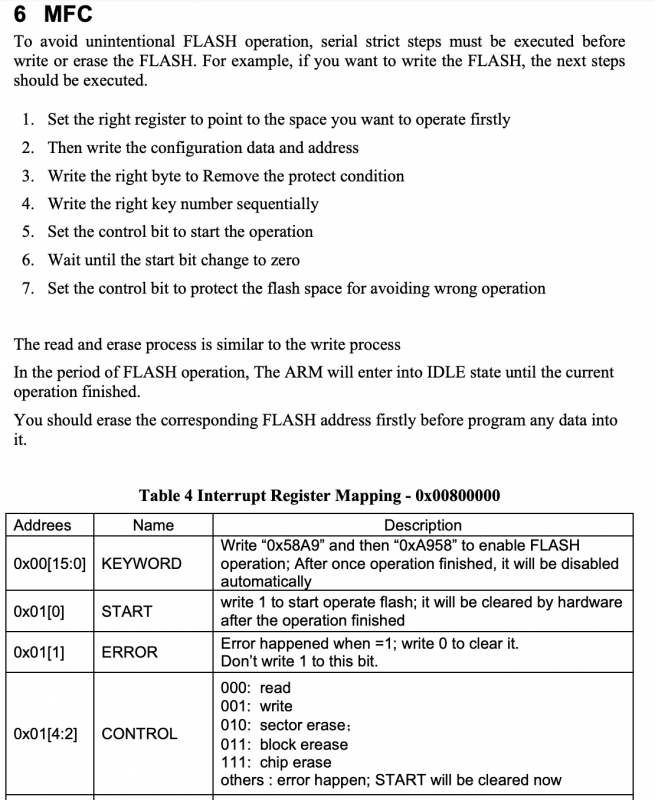 (see the rest of the registers on the PDF itself) How would you approach this? Last edit by brainstorm at 19 Jul 2020, 01:46 PM ------------- |
| [top] | |
| mit | Posted: 19 Jul 2020, 01:59 PM |
|
yeah whatever Admin Posts: 687 Joined: 4-May 16 |
It sounds like the MFC is just for self-programming the flash from the internal program, like you surmised. It's fairly typical to have that sort of elaborate mechanism to prevent accidental writes. Looking at the other thread I expect the registers for the SPI are also only for use by the internal program, and aren't going to be helpful for dumping the flash. By the sound of it, when the PPROG pin is enabled, the chip starts to behave as a dumb SPI flash chip. The datasheet doesn't give any details about the protocol, but many SPI flash chips behave in the same way. You could try finding a library for an SPI flash chip and seeing if it works. Another thing - in your scope picture, the MOSI line looks wrong. That shape it has, where each high bit is followed by an exponential decay, suggests one of the pins isn't configured correctly. Possibly you need to set it as output in the arduino code? ------------- |
| [top] | |
| brainstorm | Posted: 20 Jul 2020, 02:01 PM |
|
@braincode Member Posts: 9 Joined: 16-July 20 |
Thanks for the pointers! I just reviewed the setup and simplified the connections a bit. I had another FTDI UART connected via USB in parallel with the Arduino board that I didn't really need. Now that MOSI signal is square:  Anyway, before trying an arbitrary SPI flash library, is there an easy way to determine if the thing I'm talking to (while PPROG is high) is a SPI flash and of which sort? Do you know some discovery library or device like the JTAGulator but for SPI? Last edit by brainstorm at 25 Jul 2020, 01:30 AM ------------- |
| [top] | |
| brainstorm | Posted: 25 Jul 2020, 01:17 AM |
|
@braincode Member Posts: 9 Joined: 16-July 20 |
For now I went for SPIMemory (https://github.com/Marzogh/SPIMemory/blob/master/examples/TestFlash/TestFlash.ino) with minor modifications (assert PPROG):
But I doubt this thing has JEDEC ID nor it seems straightforward to read all flash via command "10":
So the return is all 0's for this one... I'll keep poking at it. I wonder if there's some sort of non-writing (safe) SPI "fuzzer" out there for this kind of discovery tasks? Or in the absence of that, which sequence of SPI commands would one issue? Last edit by brainstorm at 25 Jul 2020, 04:18 AM ------------- |
| [top] | |
| brainstorm | Posted: 25 Jul 2020, 06:22 AM |
|
@braincode Member Posts: 9 Joined: 16-July 20 |
Naively sending incrementing commands:
Returns all 0's... a validation that SPI is still working and I've not gone wrong with the wiring? ;) 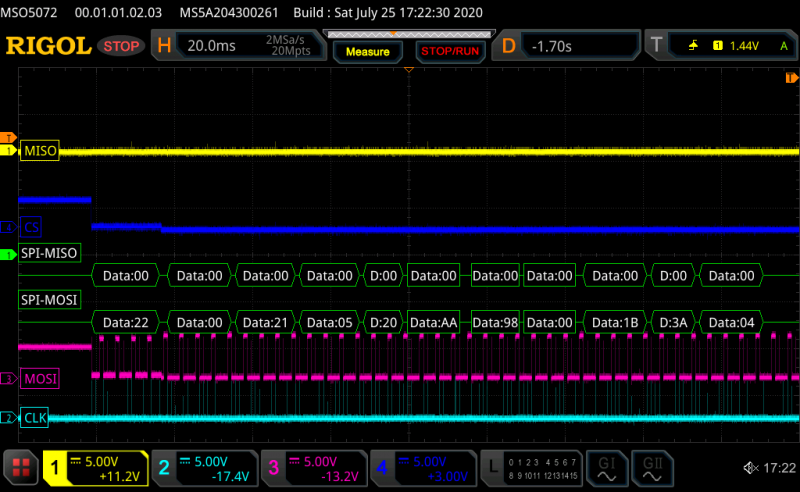 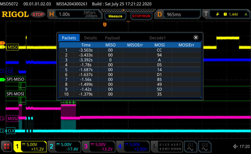 Last edit by brainstorm at 25 Jul 2020, 07:01 AM ------------- |
| [top] | |
| diizuka | Posted: 18 Sep 2020, 07:06 AM |
 Member Posts: 12 Joined: 18-September 20 |
I think SPI clock may be too fast. In another BEKEN chip specification says: The SPI clock rate is from 50.8 kHz to 6.5 MHz when acts as master, and http://c-chip.com.cn/userfile/productPic/20181201113210.pdf Last edit by diizuka at 19 Sep 2020, 03:54 AM ------------- |
| [top] | |
| diizuka | Posted: 18 Sep 2020, 10:13 PM |
|
Member Posts: 12 Joined: 18-September 20 |
I found another BEKEN chip BK7252's tool's code. https://gitee.com/withome/bk7252_RTT.git On beken378/driver/spi/spi_flash.c, serial Flash memory commands are defined. Read command is 4byte length (0x03, addr_upper, addr_middle, addr_lower) But.. this code may be for BK7252's internal SPI, not for flash reading/writing from outsite. Last edit by diizuka at 19 Sep 2020, 02:09 PM ------------- |
| [top] | |
| diizuka | Posted: 19 Sep 2020, 02:06 PM |
|
Member Posts: 12 Joined: 18-September 20 |
It seems like to be BK3231 firmware image, but download link is 404. http://www.codeforge.com/read/303932/program_flash.sh__html How about this one ? I googled "BK3231_flash_image.bin" and find it. https://github.com/AriesTian/BM3231 Last edit by diizuka at 19 Sep 2020, 02:15 PM ------------- |
| [top] | |
| brainstorm | Posted: 28 Sep 2020, 12:55 PM |
|
@braincode Member Posts: 9 Joined: 16-July 20 |
Wow, thanks for all that search and info, that could keep me busy reversing those .bin for a while! :D Did you try any of those SPI commands yourself on a real BK3231 IC? I might do the setup again and try myself... PD: @Mitxela, this forum shall (if it doesn't already) have some sort of notification mechanism, RSS or Email... I almost missed those great reponses :) ------------- |
| [top] | |
| mit | Posted: 29 Sep 2020, 10:58 PM |
|
yeah whatever Admin Posts: 687 Joined: 4-May 16 |
QUOTE
PD: @Mitxela, this forum shall (if it doesn't already) have some sort of notification mechanism, RSS or Email... I almost missed those great reponses :) I never got around to making this forum give email notifications. I've been meaning to add it, will try and do it soon. ------------- |
| [top] | |
| diizuka | Posted: 2 Oct 2020, 04:38 AM |
|
Member Posts: 12 Joined: 18-September 20 |
I have some BK3231 board(JDY-30, JDY-31). I wish to try to read firmware, but currently I have not time to do it. BK3231 VDD is 3.3V, but Arduino VDD is 5V. Does your BK3231 still working ? ESP8266, ESP32 are working on 3.3V, so is better to do it. I found some hints for writing Beken firmware. These are not BK3231, but it may be informative to us. Writer and wiring to BK3431S dev board (See fig.2) https://item.taobao.com/item.htm?spm=2013.1.w4004-14948376696.7.5391340b6T2bRi&id=537588483657 BK3431S Dev board wiring diagram (See fig.2. Fig.1 is BK3231S, not BK3431S) https://world.taobao.com/item/555113287141.htm BK3431 dev diary in Chinese. Table left side is writer pin, right side is core pin. https://cloud.tencent.com/developer/article/1689680 https://cloud.tencent.com/developer/article/1689683 WireColor, Writer, BK3431S, Function(estimated) Orange, WP, WP, Write Protect? Red, VPP, VDD, Gray, GD, GND, Pink, HOLD, HOLD, High: Flash in program mode Purple, SO, SO, MISO Green, CS, CS, Yellow, SCK?, SCK, Blue, SI?, SI, MOSI BK3231 has VDD,GND,SO,SCK,SI. And PPROG, PRSTN(Reset?) According to the general SPI flash manual, WP=High, HOLD=High, CS=Low seems to be required for writing. The problem is: 1) Where are WP, HOLD, CS are connect to BK3231 pin ? 2) How to treat PPROG and PRSTN ? In my estimation, HOLD - PPROG, CS - PRSTN. WP - Somewhere of GPIO. To start writing, let CS high in a while and then low (i.e. reset), like ESP32 GPIO0/GPIO2 boot mode selection. Last edit by diizuka at 2 Oct 2020, 05:08 AM ------------- |
| [top] | |
| mit | Posted: 3 Oct 2020, 12:25 AM |
|
yeah whatever Admin Posts: 687 Joined: 4-May 16 |
Hi brainstorm, I've now implemented email notifications when someone replies to a topic you've posted in. Let me know if you have any feedback. ------------- |
| [top] | |
| brainstorm | Posted: 3 Oct 2020, 07:58 AM |
|
@braincode Member Posts: 9 Joined: 16-July 20 |
It works, thanks Mitxela! :) ------------- |
| [top] | |
Sign in to post a reply.