
Smallest USB-C MIDI Synth
15 Dec 2023Progress: Complete
A new entrant in my series of "smallest and worst" MIDI synthesizers. (I'm not including the flash synth in that list, which isn't supposed to be the worst!)
Here's a video of the creation:
Story
The last few weeks I've been dabbling around with the CH32V003, a 32-bit RISC-V microcontroller that's unbelievably cheap.One of the first things that occurred to me, when I noticed it didn't have hardware USB but the processor is clocked at 48MHz, is that it would be awesome to write a software USB stack for it. I have wanted, for a long time, to dig deep and write a bit-banged USB library, just because it's the best way to learn. I greatly enjoyed writing my ethernet bootloader in assembly. It's hard to justify writing a USB stack from scratch when one already exists, however, so when I saw the CH32V003 I thought this was the perfect time to do something both educational and useful.
Picture my surprise to find that CNLohr has already done it! I can't exactly complain, that's a fantastic achievement and makes the chip even more useful and impressive than it already was.
The very least I can do is get some USB-MIDI working on the chip. At the time of writing, the USB-MIDI demo was unfinished, so I tried it out by soldering a dev board together. It started out a little smaller, but by the end of the experimentation my board looked like this:
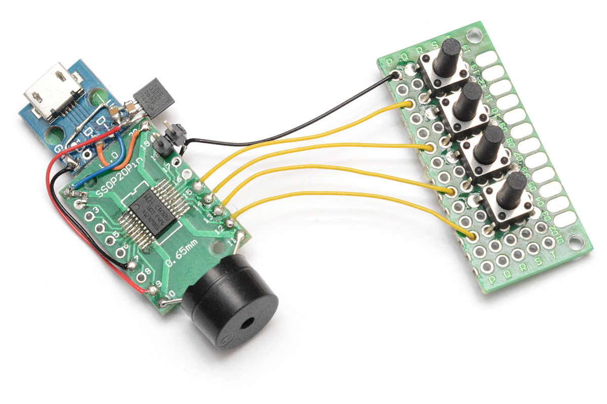
That's a TSOP20 breakout and a Micro-USB breakout, superglued together with some other scrap circuit board. A regulator, capacitors and a few resistors complete the circuit. The two header pins are my programming header (though with the USB plugged in, we don't even need to connect the ground pin, and could get away with just one pin to program).
On the right is a set of buttons. I configured the USB-MIDI device to play notes when these buttons are pressed.
At the bottom is a piezo buzzer. Naturally, when MIDI data arrives at the chip, it produces a square wave. I did this with one of the hardware timers of the chip, outputting in differential mode to maximise volume.
USB MIDI messages are four bytes, and our low-speed USB endpoint can be eight bytes, so we could (and normally would) send two MIDI messages per packet. However for this simple demo I just blocked until the next USB interrupt for each message.
A bit of MIDI loopback on the host side, and we have a really terrible toy keyboard!
USB dev board
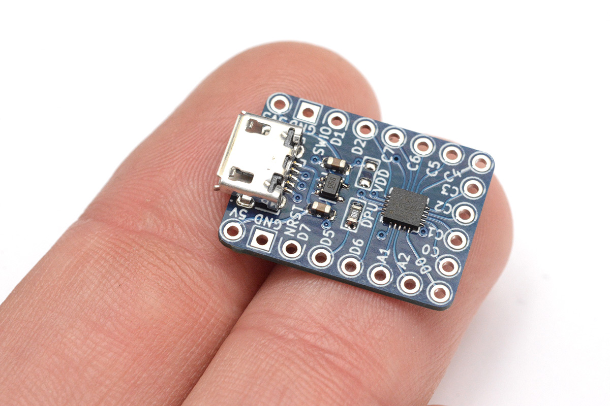
There are a few dev boards available for the CH32V003, but it doesn't look like any of them wire up the USB pins, probably because there's no hardware USB. I doubt this is the last USB project I'll do with it, so to avoid having to repeatedly wire up that mess above, a simple dev board is in order. I tried to make it as small as possible.
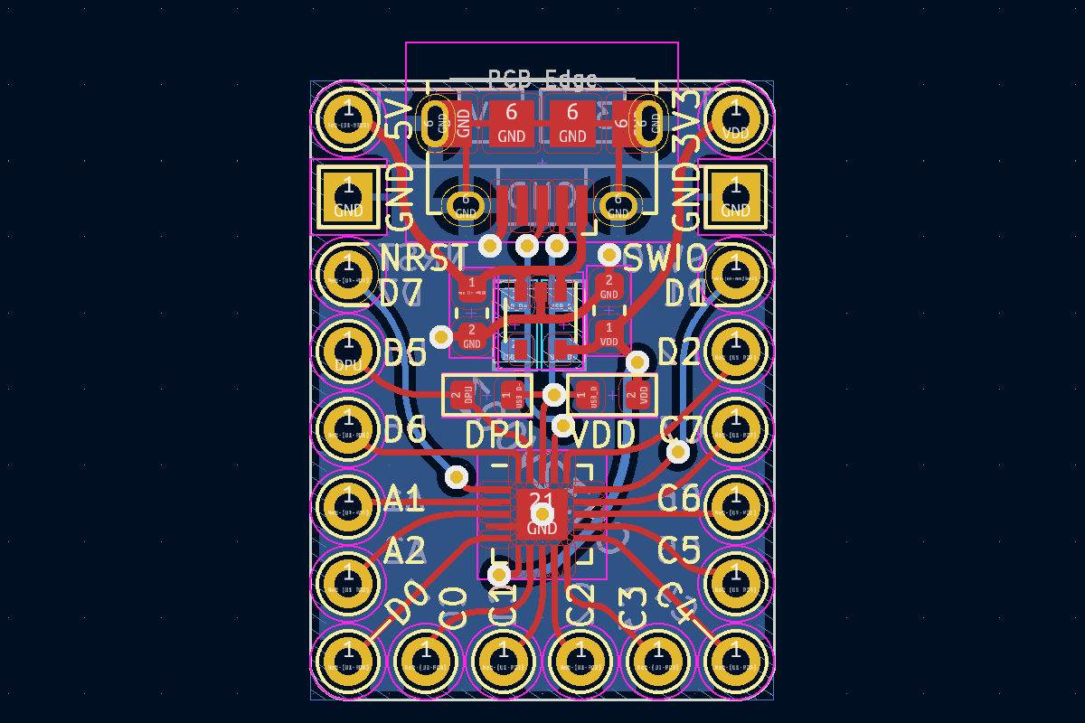
All the necessary pins are broken out, all pins are labelled on both sides. The 1.5K resistor can be soldered in one of two positions, either to D5, or direct to VDD if you don't need software reconnection of USB and want to use D5 for something else. On the underside, the USB data lines can be cut and series resistors can be added, if needed.
The three pins in the top right corner are 3V3, GND and D1, which is what I've been using as a programming header. You can either connect all three (to program it with USB unplugged), or D1 and ground, or just D1 if the programmer is on the same machine that the USB is plugged into.
The pins around the edge are .1 inch pitch, and the board is 15.2mm by 20.3mm total.
Here's the obligatory 3D model of the board:
The KiCad design files for this board are published here and here.
More USB, all the USB
Given how cheap the part is and how few supporting components it needs (the USB stack even does the same oscillator calibration frame timing trick that V-USB does), I thought it might be fun to recreate some of my USB ATtiny projects.The stylocard comes to mind first. I've done a few unpublished redesigns of that board in the past, and the best improvement was getting rid of the analog input method which was a little unreliable once the thing got dirty, and switching to direct readout, which means a microcontroller with at least 22 GPIO. One day I should publish all that. Unfortunately our CH32V003 doesn't have enough pins to read the keyboard and do USB together.
We could just go with the same as before, a bunch of resistors and make the reading analog, or we could try and do something clever, or even just add a shift register, but it then occurred to me that since the CH32V003 is so cheap, why not just stick two of them on the board? It would be hilarious. One of them could read half the keyboard, the other would read the rest and also do USB.
The possibilities are not unlimitless!
Recreating my smallest USB MIDI synth was the next thought. Something I've wanted to do for a while is produce a thin circuit board as they do for some dongles, sliding the thin circuit board inside of the USB-A plug, essentially creating the circuit I did before but in a way that can be mass-produced and easily assembled.
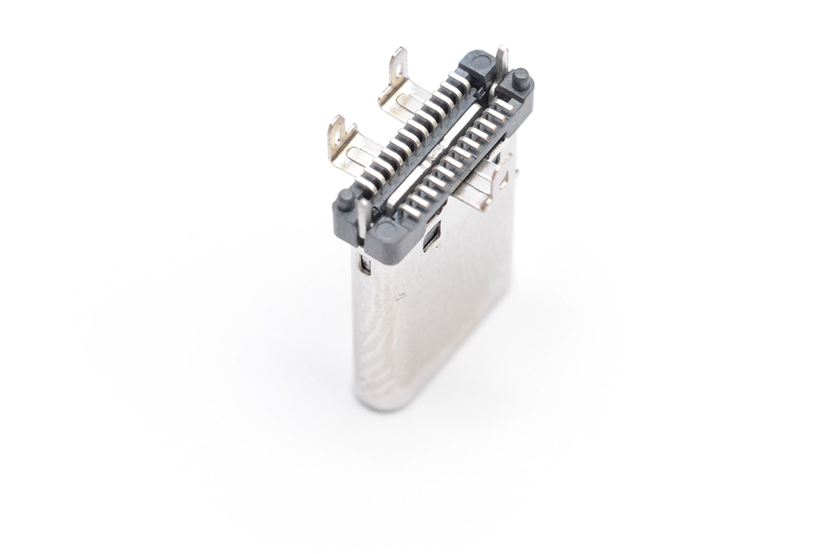
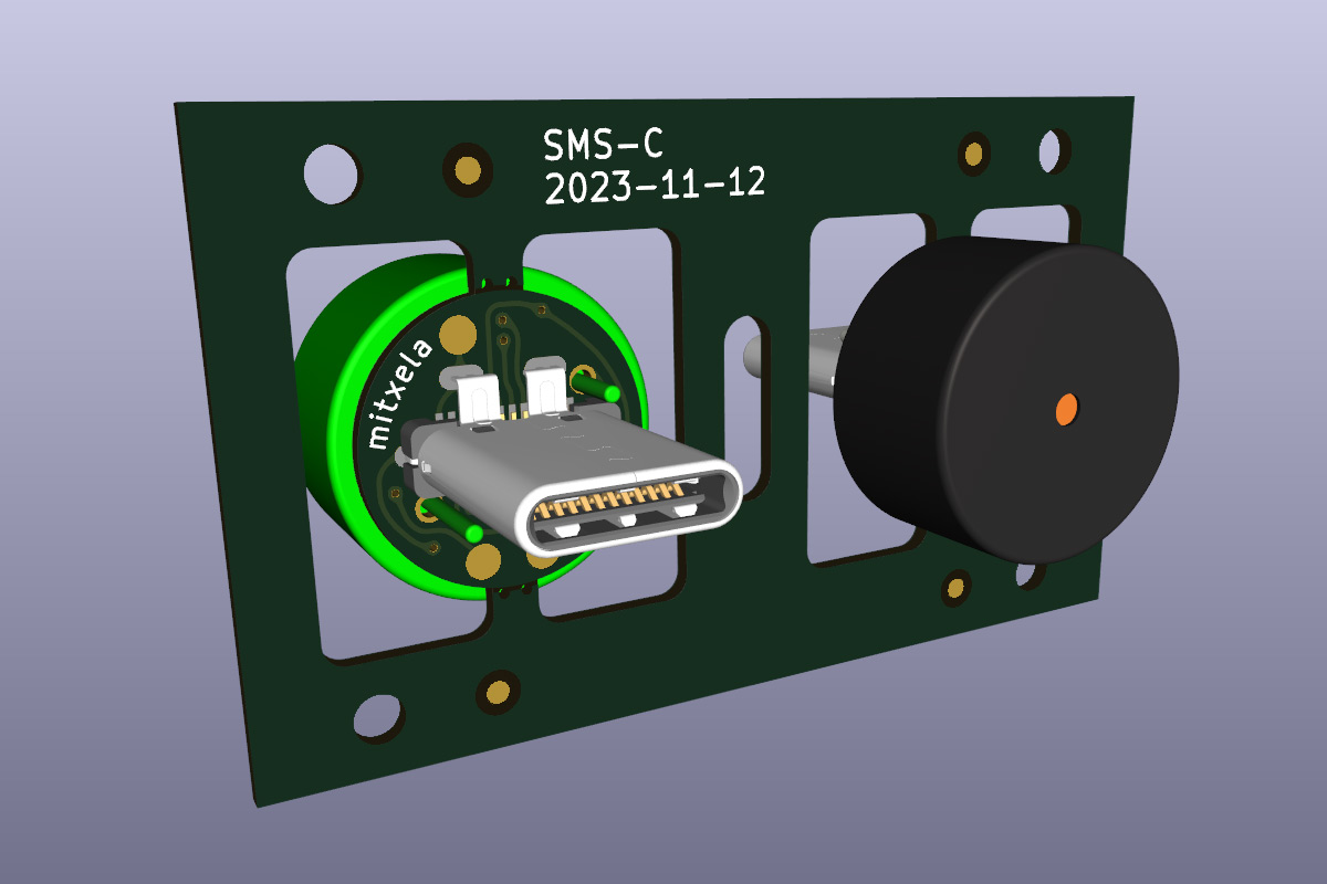
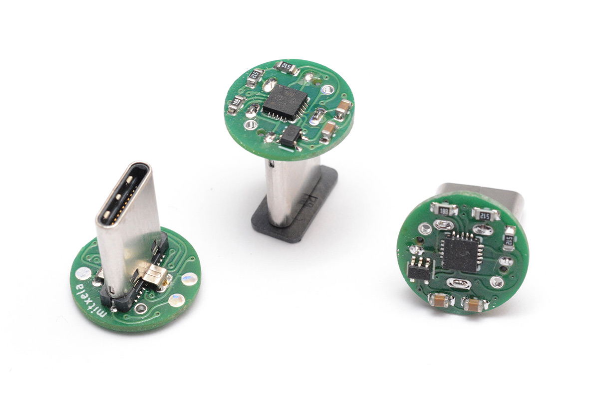
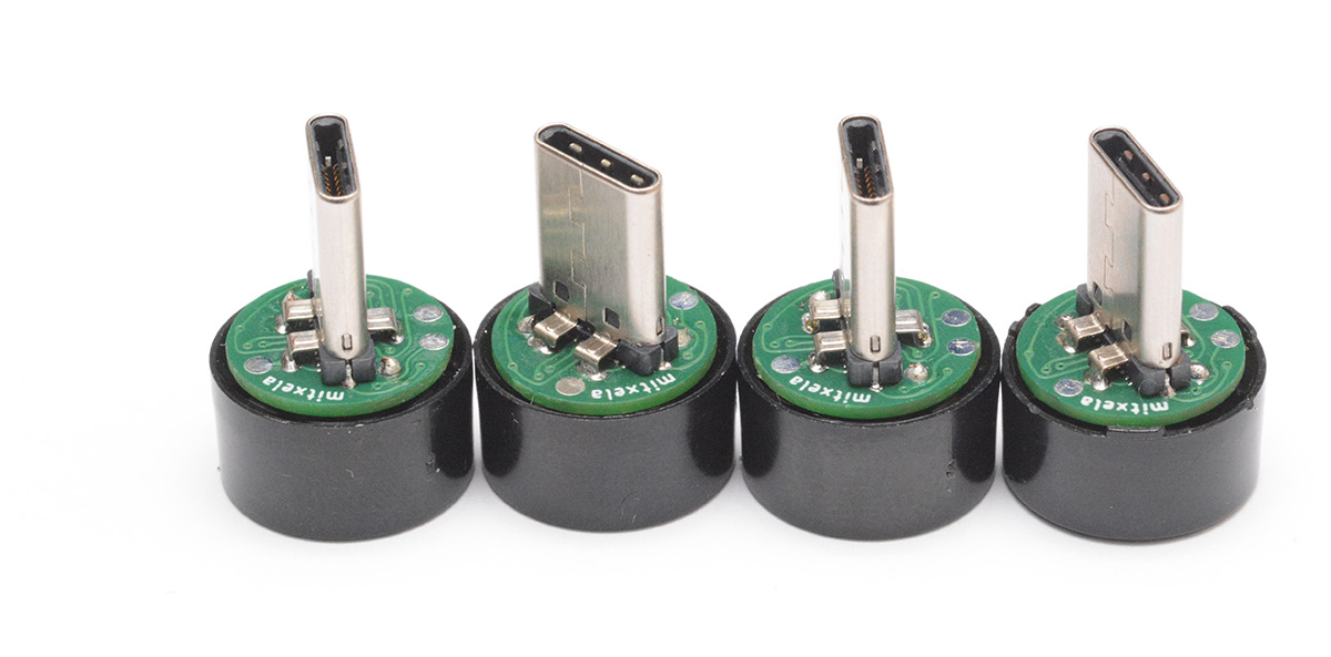
But a more interesting idea was to bring the synth forwards through time into the age of USB-C. Electronically this just means adding a couple of resistors and fitting the right connector. You can't mount electronics inside a USB-C plug so easily though. I did find some mid-mount USB-C plugs which may have worked, but after a bit more searching I settled on this vertical mount type, intended for building docks.
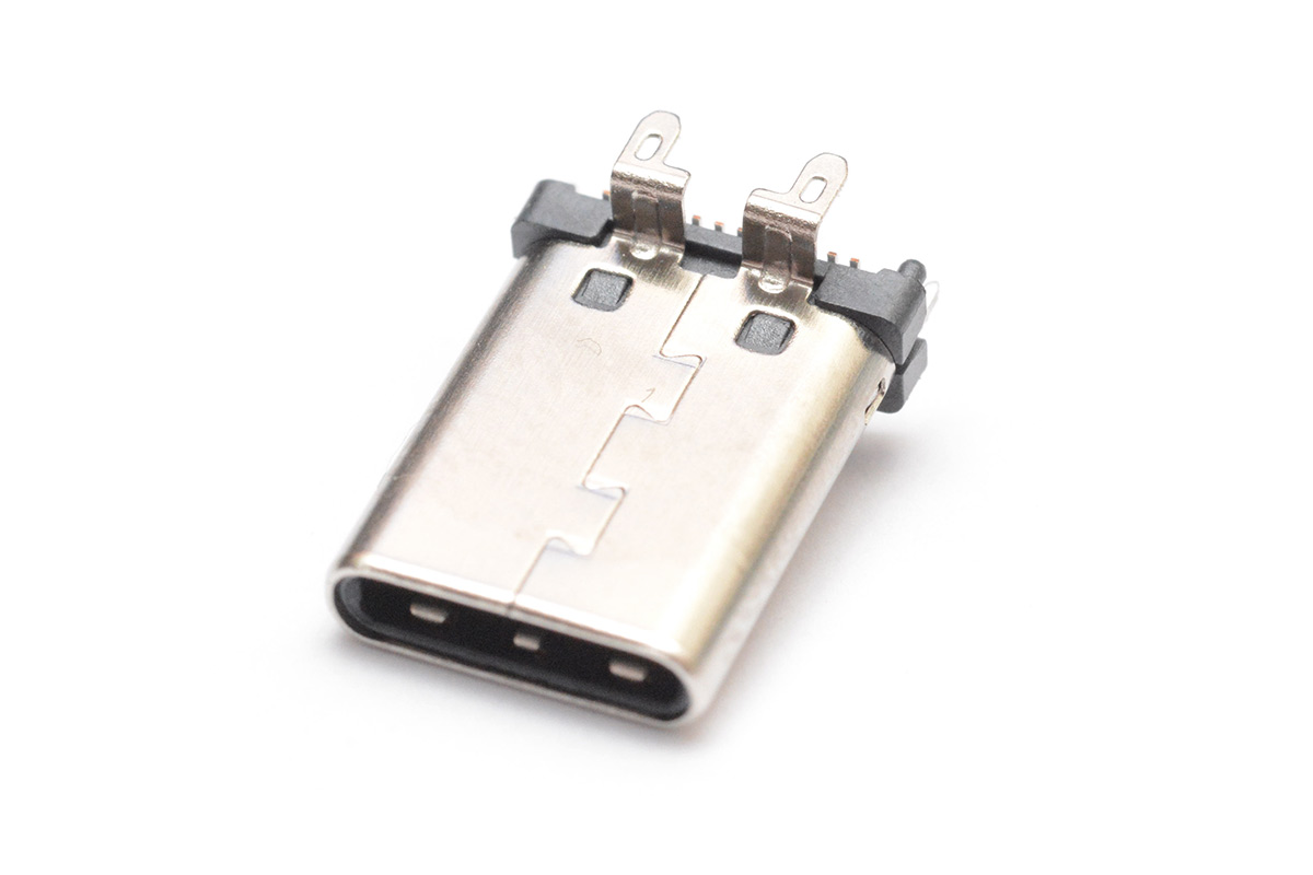
The part number is USB4151 although there are a few similar parts from different suppliers.
When USB-C was introduced, a lot of engineers complained about the difficulty of fanning out the connections. It seems the designers of the connector assumed that everyone would be using high density boards with microvias. The footprint alone of this connector is technically beyond the spec of a standard 6/6mil process, and that's before we've added any traces.
The plastic studs require a non-plated through hole in very close proximity of a plated hole. For this joke project I'm not going to pay for tighter tolerances, so I decided to just ignore the DRC violation and if they aren't able to manufacture the holes I can trim off the plastic studs with a knife.
The difficulty of fanout on a two layer board is such that special USB-C connectors are available, that don't break out all of the pins, if all you need is USB 2.0 or just power. However, they're not available in this vertical format, and besides I eat tricky routing problems for breakfast.
Routing
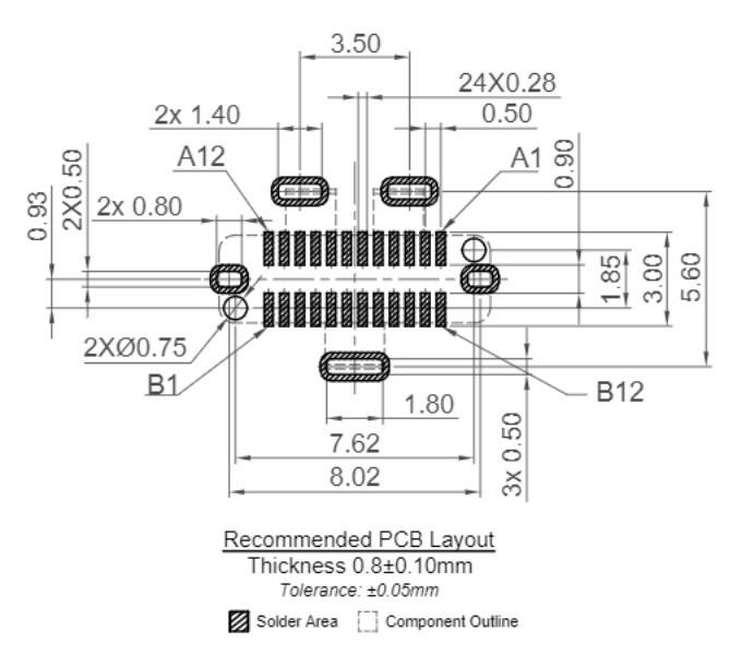
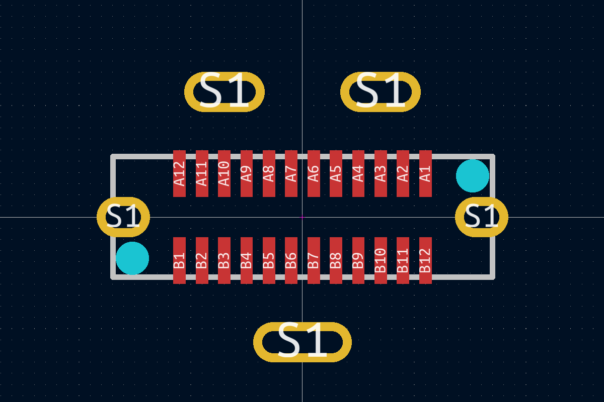
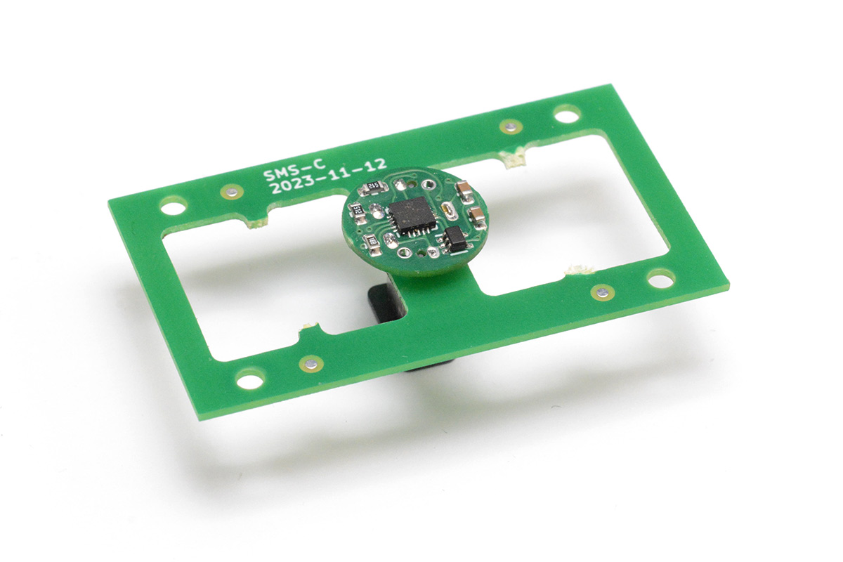
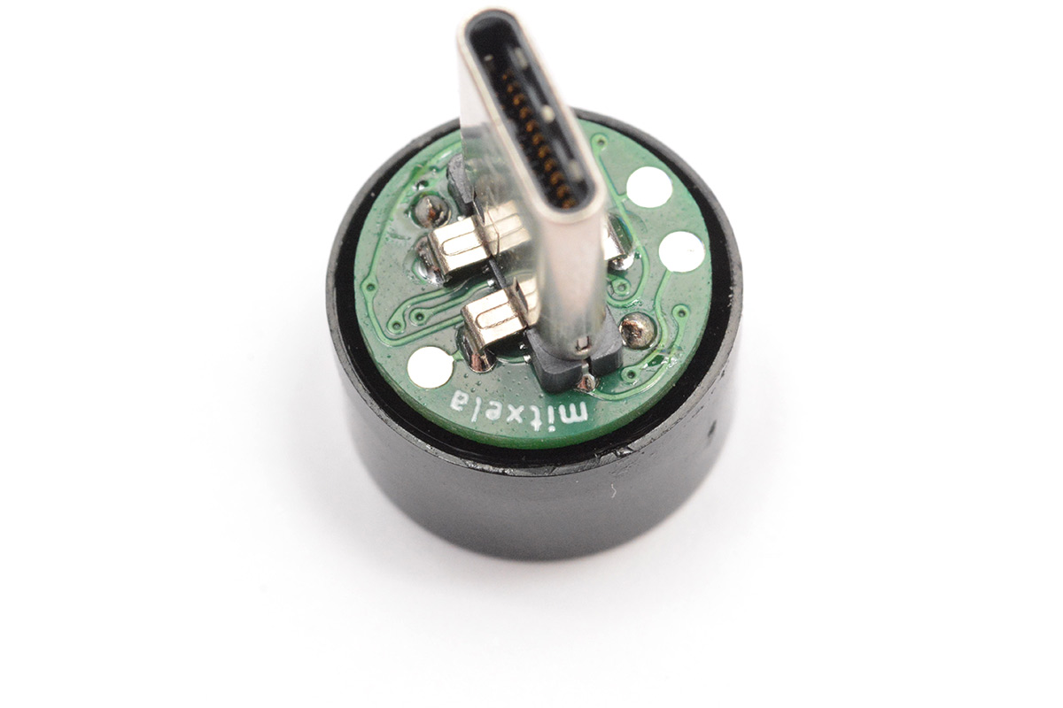
With the vertical-mount USB-C plug, our ambition is to make the smallest possible circuit board underneath it, that can fit within the diameter of an ordinary piezo buzzer. The buzzer has a pin pitch of 7.62mm, or 0.3 inches, and the outer diameter is 13.8mm, but we want our circuit to fit inside the depression, that meniscus of the potting compound, which means a maximum diameter of about 12mm.
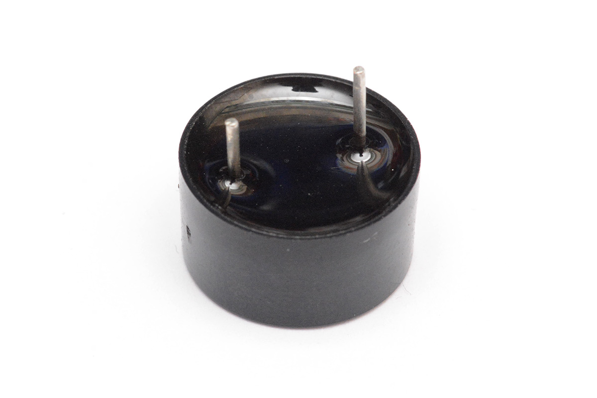
There's no possible orientation where the piezo's pins don't foul the USB support pins. To deal with this, I widened the footprint spacing. It should be fine to bend the pins outwards a little, but if it doesn't fit we can file them down too. As the design iterated, I reshuffled this a few times, eventually I got them down to just 8mm apart.
We don't need to connect the USB 3 pins, that's the four superspeed pairs and the two SBU pins, but we do need to wire up CC1 and CC2, which totals 14 pins to connect. Keeping the copper annulus around each plated hole as small as possible, it's just possible to have all the necessary tracks escape.
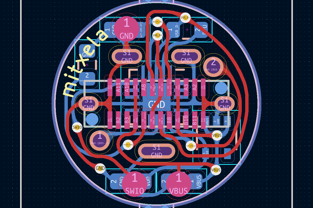
Naturally the tracks are rounded with teardrops, because I have standards to live up to.
As the shielding pins are all connected, we could cheat and not connect the grounds together on the board, but in the end it was fine to route these all together too.
On the underside, routing is just as tight, with the QFN part shoved off-centre to make enough room for the tracks. Thankfully it doesn't hurt if we connect unused GPIO to ground (or to other signals really), so we can conveniently route ground right through the middle of the chip instead of going around.
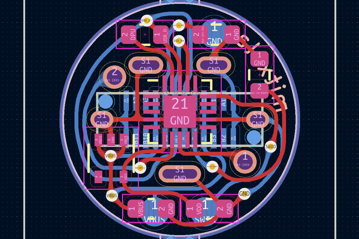
The regulator is an SC-70 package, that's like the miniature version of SOT-23. You can get even smaller regulators but it didn't seem like it would be an issue. Similarly, around the periphery I've used resistors and capacitors in 0603 format, just because there's no real pressure for space once we're outside of the piezo/USB/QFN footprint mess.
On the front side I put three test pads, for power, ground and D1 (SWIO) for programming. In reality only one pad is needed, I'm just going to plug the USB-C in with an extension cable and touch a single wire to the programming pad.
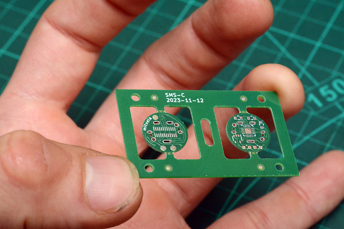
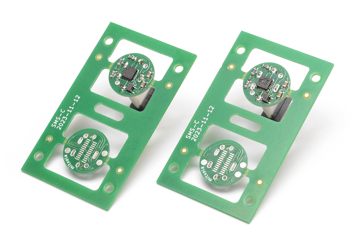
Panelization
I wanted to do the panel myself for three reasons.When you get boards made that are this small, and you plan to stencil solder paste onto them, it's extremely fiddly to hold things if you don't have a frame. A 12mm circle would be very tedious to hold at the best of times, but here we have components on both sides so after one side is soldered it'll be almost impossible to stencil the other.
Secondly, I specifically wanted the panel to have explicit symmetry. We use the frame and the mounting holes to align the stencil. To save on the tedium of doing this twice, I put down two copies of the design, with the second flipped over. The whole panel is symmetric, so we can stencil one side, flip the board and stencil the other.
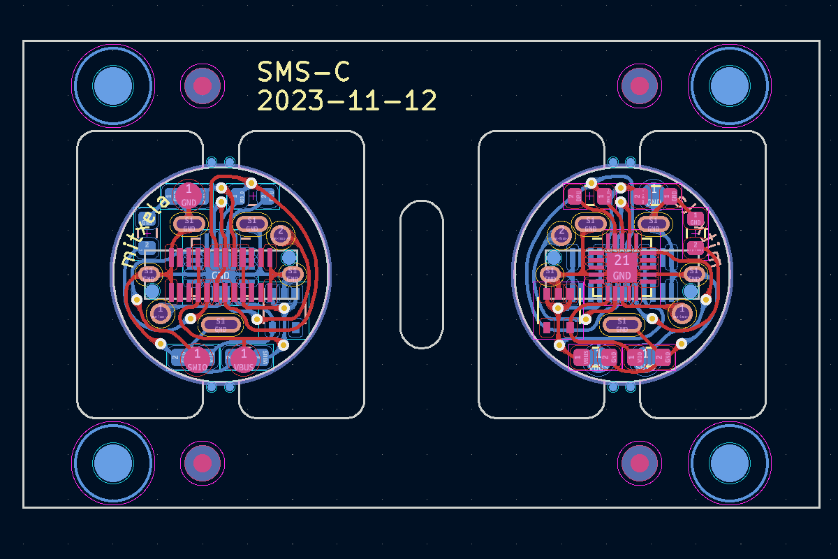
The third reason to do the panel myself is that I wanted to also use the frame as a jig. There's an oval hole in the middle designed to be a tight fit around a USB-C plug. Once the board is part-soldered and broken out of the panel, it's going to be a real pain to do anything to it, so this at least should give us a basic grip on the thing. We could have made a jig ourselves out of something else, but there aren't many materials that can be laser-cut and would survive the reflow oven. In a sense, FR4 is the perfect support material.
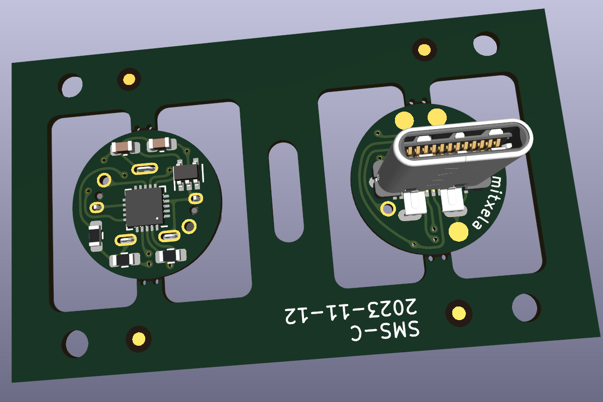
I should take this moment to praise just how useful the 3D model viewer is. I can remember once having a bizarre argument with a contractor who was a little old-school and failed to see the benefit of it. He'd grown up with OrCAD in the 90s and insisted that setting up 3D models for part footprints was a waste of time, or at the very least, not his job. 3D modelling is for the mechanical engineer, he kept saying.
But being able to look at a realistic render provides such a huge safety buffer against silly mistakes. In the old days, we used to spend hours poring over gerber files looking for common mistakes because if you made one, it could set everything back by weeks. And they happened all the time! Things like missing the soldermask aperture on a footprint, or exporting shapes onto the wrong layers. Ever since we shifted to KiCad and made full use of the 3D viewer, I don't think I've ever made one of those mistakes. I still check the gerber files religiously, but the 3D viewer is a second layer of defence against mistakes.
In the render below, I've highlighted the piezo, and you can immediately see that the pins don't quite line up with the footprint. This is because I've intentionally altered the footprint in the hope that we can bend those pins outward a little, as mentioned above. But it's exactly the kind of thing that the 3D viewer can help you with, to get a visual on the interference and whether it looks like it's going to work. Or at the very least, it might make you go back and check the 3D model is correct.
Here's an interactive 3D model if you're especially keen:
Assembly
If you get your boards made at the lowest tolerances and they're below a certain size, manufacturers will subsidise the price. It's essentially a promotional deal, they charge you almost nothing because it costs them almost nothing to chuck tiny boards into the corners and crooks of other panels. I wonder how many other people have tried to produce a board with a (nominally) USB 3.2 Gen 2 connector on a two layer, 6/6mil tolerance board.
They didn't question my footprint at all, and it seems to have been produced without problems.
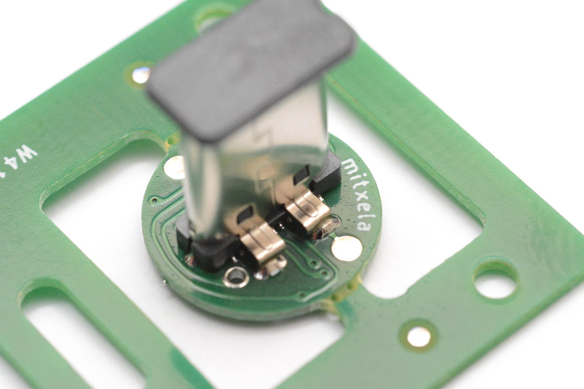
The correct order of assembly is to do the tiny parts first, and the USB connector last. The through-mount aspect of the USB connector means it's not possible to stencil the other side once it's fitted.
The USB connector comes with a plastic cap, to allow you to pick it up with a vacuum nozzle.
I had planned to reflow a bunch of these, but it's so small I ended up doing all of them with the heat gun. It's possible (and not that unusual) to reflow a board with components underneath already soldered. Even if the solder melts, surface tension holds them in place. It's also possible to use two different alloys of solder with different melting points if it's a concern. But hitting it with the heatgun it's easy enough to direct the heat only to where needed.
If I had reflowed it though, the plan was to stencil and place components on both sides, then reflow the whole thing at once. Something like the following picture:
The connector itself would poke through the grating that makes up the bed of the reflow oven.
Anyway I didn't do that, I just soldered them all in place as it was way less tricky than I'd imagined.
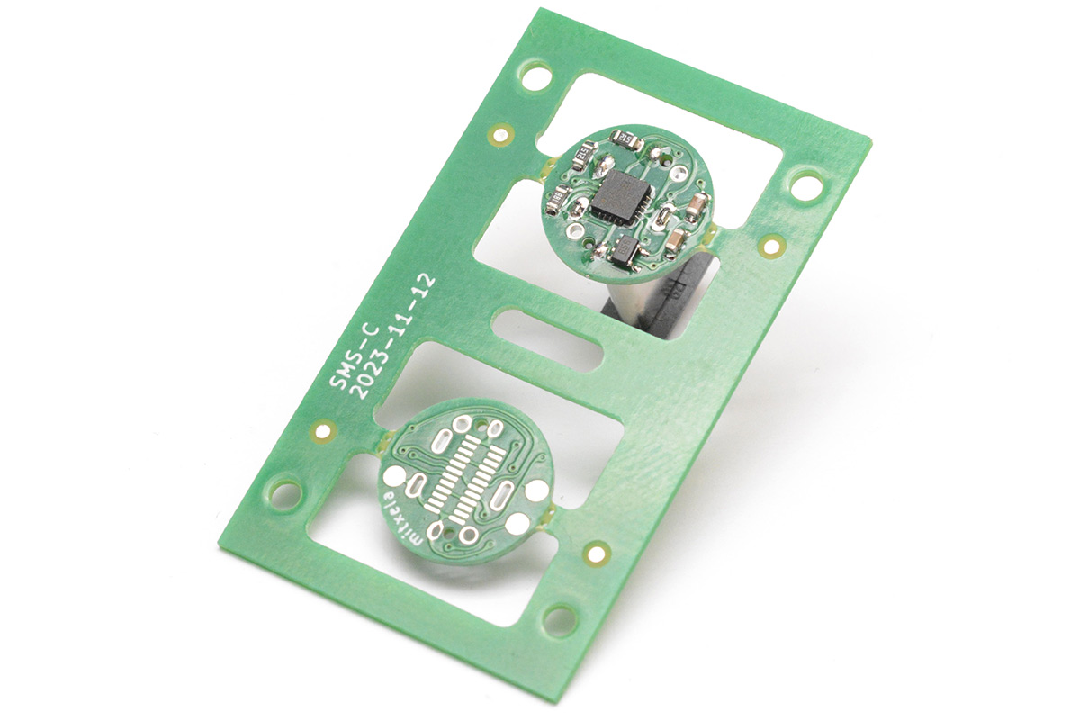
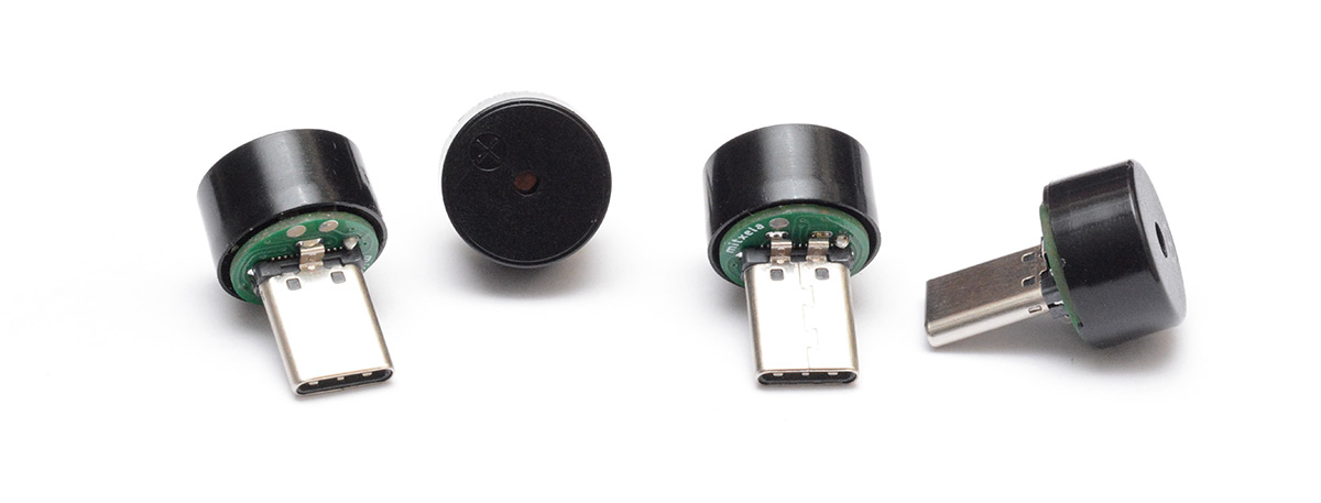
Carefully snap them out of the panel and file the rough edges a little.
After assembling them, I did wonder if perhaps I should have gone with smaller capacitors after all. They're the tallest single components, and smaller caps are easily available. Oops, too late now.
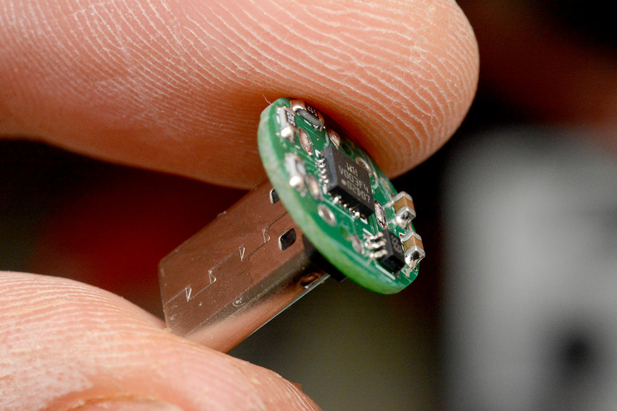
As expected, the buzzer pins were a tight fit, but there was enough play to jam them into place and get the board flush. I then trimmed them to length and delicately soldered the stubs.
Comically I waited until this moment to realise I didn't have enough piezo buzzers in stock. I ordered some more and the new ones are a minutely different design, which was inevitable. Never mind.
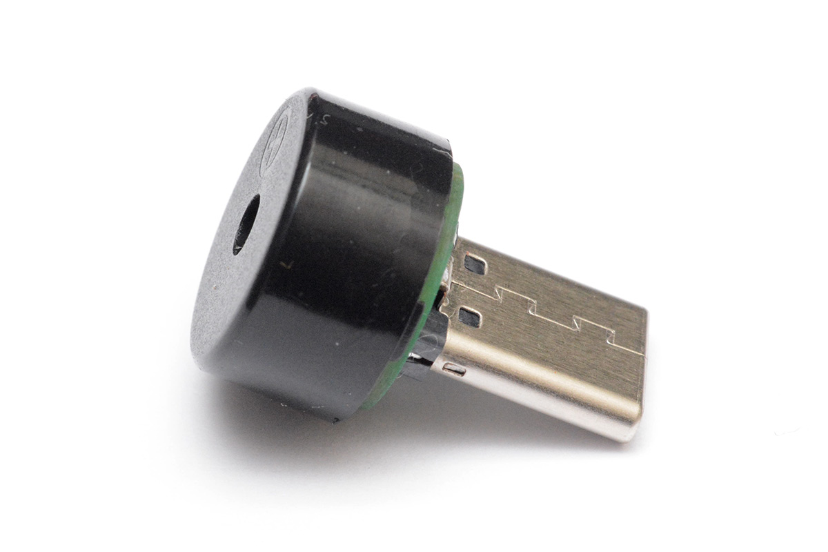
That vertical-mount USB-C connector was designed to go inside a dock for a phone or tablet. It's supposed to poke through a moulded plastic case, which means it's a little longer than it needed to be. I did have a think about 3D printing a little plastic cover to go over the circuit board and the lowest part of the connector, but I doubt it would look very good. We wouldn't want to cover that mitxela logo anyway.
USB-C extension cables are technically against the spec, but that doesn't mean you can't buy them and all kinds of other nonsensical cables and connectors. I have one that only works in certain orientations, which is just so distressing and the opposite of what USB-C was supposed to be, but it'll do to give us power while I poke that SWIO pin with a probe. I flashed the four different synths with different device names, which helps us differentiate them in a DAW. And by DAW I mean the 1998 edition of Cakewalk running in wine.
I then went out of my way to buy a four-port USB-C hub. Surprisingly difficult to find, most of them turn USB-C into various more helpful connectors like USB-A, HDMI, SD card, and so on.
I have a bunch of the PCBs left, maybe I should make another handful and get even more hubs?
Interestingly the design works with the hub, and it works if I plug it into my phone, but it doesn't enumerate if I plug it straight into my laptop. But it does enumerate on the end of that noncompliant USB-C extension cable I've concocted. It's entirely possible I've wired up the USB-C port marginally wrong, or perhaps the resistors are not exactly the right value – the type of USB connection is determined by the strength of some of the pull resistors. Either way I don't think I care enough about this comedy synth to look into it much further. It's just something to keep in mind for the next USB-C device.
I have put the source code for this project in the usual places.