
RC Transmitter USB Joypad Mk II
29 Mar 2017Progress: Complete
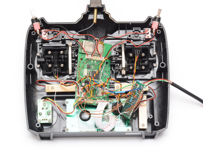
Didn't think I'd be building a mark II so soon, but a friend of mine with the exact same transmitter commissioned me to repeat the mod. To be clear, there is nothing wrong with the first edition of the RC TX USB Joypad, but since we get a second shot we might as well do it right this time. We want the same functionality, but lower power usage and a simpler design.
Last time I was under extreme time pressure and cobbled together a mess from what I had, but now we have the luxury of ordering parts and waiting for arrival. First thing is to get hold of a microchip that suits the bill. Essentially we need an ATtiny85 but with more pins. I really like the PLL clock source option on the tiny85, and if we look for other AVR chips that have it we're limited to just a few. The ATtiny861 sounds like just the ticket, with virtually the same specs as the tiny85 but in a 20-pin package. This, along with a few passives to fire it up, should be the only IC we need to add.
The other part I ordered was a switched-mode 3.3v regulator. In fact the buck regulator I ordered is an adjustable type, you just set the trimpot to the voltage you want. It's suitably tiny, but the main concern is whether the output ripple is low enough to not affect our analog readings. After setting it to 3.3V, I gave it a load that drew maybe 50mA and watched the ripple on the scope. Generally, higher quality switched-mode supplies use higher frequencies and hence smaller inductors. This is not a particularly high quality one. The ripple was pretty bad so I added a simple low-pass filter.
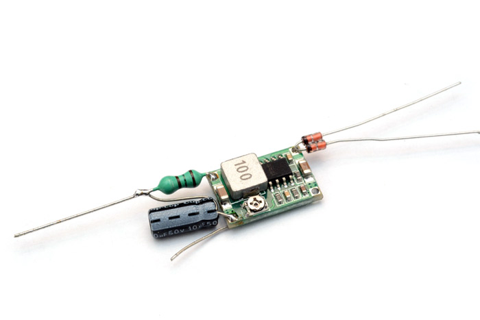
It's an LC filter, of course we don't want to put a resistor in the path from the power supply. The green thing is a 100 μH inductor. The two Schottky diodes on the input are the voltage selector, one will be from the battery and the other from the USB supply.
But we have to be careful with a reactive load. Too much capacitance can cause instability in the output voltage, and when I tried adding a second stage to the low-pass filter it actually made the ripple worse. I don't have a big selection of inductors, so that single filter will have to do.
On the main board for the transmitter, I ripped off the linear regulator (just cut the legs, it's quickest) and soldered wires to the input, output and ground.
I wired up the new buck regulator and found that it didn't work at all. So, it turns out the transmitter draws between two and three hundred milliamps and my dummy load for it was completely inaccurate. The dropout voltage for the power supply at that current seems big enough that we can no longer power it through the USB and diode. Bugger. This was meant to be a simpler design.
Well, scrap the SMPS then. I grabbed a brand new 3.3v linear regulator and soldered it onto the original pads. It's inefficient, but it functions and is simple. Reducing the power consumption during ordinary usage would have been nice, but not a must-have. I also decided to scrap the diodes. Instead, we will perform what we should have done to begin with – physically switch power sources.
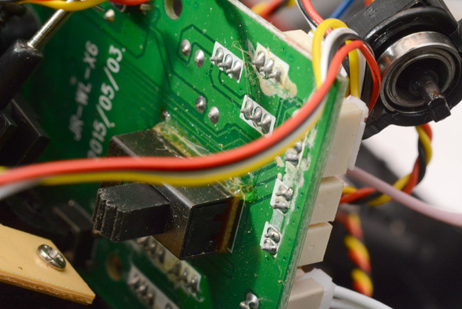
The on/off switch on the transmitter is a double-pole, double-throw. But it's wired in the most confusing way, trying to support an unpopulated feature, labelled on the board as 'DC IN'. The battery voltage is exposed to the centre terminals, in the 'on' mode it connects to the linear regulator and supplies the device, in the 'off' mode it's connected directly to the DC-in socket on the board. Presumably you'd fit the transmitter with rechargable batteries and connect your charging voltage to it. By the way, there is no barrel jack or anything on the case.
With a double-throw switch, we could connect the regulator input to the centre pin, and have the other two pins as the power sources to select. This is clearly the optimal solution, but it means cutting all the traces to the switch on the board, and rewiring it completely, without damaging the mechanical stability of the switch which is only supported by the solder joins to the board.
There are traces that need cutting on both layers, since the switch pins are used as vias. To get to the underside of the board, we need to remove the potentiometers sticking out of the joystick bearings. This is particularly fiddly for the throttle stick, which is clamped by the spring pressure, but once all the screws were undone I was able to get a look at the underside where the switch is mounted.
In the top right of the picture is one of the potentiometers, which are actually quite high quality. The need to be very low friction in order for the sticks to quickly spring back when released.
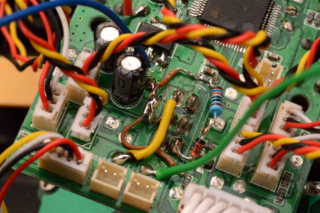
There are two traces to cut on the underside, one to the battery connector and one leading away from the switch to a via. On the top side there were three traces to cut, although the one to the DC-in jack probably doesn't matter. Then, we need to add jumps to restore continuity between the sections we just cut while keeping the switch isolated.
In the picture below, I've soldered a regulator back in, cut the traces, and put jumper wires between the sections that need to see the input voltage. The bottommost part is the current-limiting resistor to the LED backlight which apparently runs directly from the battery, I suppose it's the only part that needs more than 3.3V. The other addition is the diode and 100K resistor that will trick the battery measurement ADC into thinking there's a non-empty battery when on USB power.
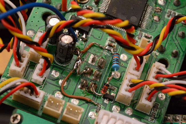
The lowest pin of the switch will be where the USB voltage connects. The top pin now needs jumping to the battery connector. (The top pin corresponding to the 'on' mark position of the switch.)
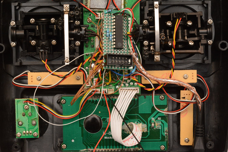
It's getting busy, but it'll get busier yet. Those test pads all around where we're working, we'll need to solder wires to them in a moment, as they're the wiper pins of the pots.
The green wire now connects to my USB cable and thankfully, the power source selection mechanism appears to work. The transmitter powers up from USB when in the 'off' position and from batteries in the 'on' position. No warning beeps, all appears to function. Great! So much simpler than the hassle we went through before.
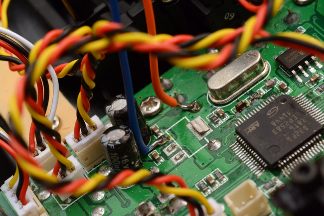
Now we can start work on the microprocessor side. We need to power the circuit from the 3.3V on the main board, but the USB pullup on the data line needs to go to the 5V coming in. That's easy enough to manage. Then four wires go straight from the test pads to the ADC inputs on the chip.
I prepared a USB extension cable to use as a panel-mount socket as before, and interestingly, even though it's the same item, from the same supplier, this one is correctly shielded and with the data lines twisted, as they're supposed to be. I stuck the ATtiny861 on a bit of protoboard, and since it has a different footprint to other chips of the same size, instead of using a test clip to program it I just soldered in place a traditional ISP header connector.
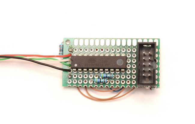
The two resistors on the data lines are probably redundant, since we're not using zener diodes to limit voltage this time, as the chip is going to be powered from 3.3V.
Now to solder the analog voltage wires, and since we have a bunch of spare pins, I wired up the switches too, so we can transmit the full eight signals over the USB line.
Ooh. Busy. You can also see that I've done a cutout for the USB socket in the lower right corner, as before.
One last bit of hardware to do. When battery powered we want the USB circuit to switch off. I think the ATtiny constitutes maybe 1% of the total power consumption, so we needn't really concern ourselves with sending it to sleep, but every little helps. While there should be a pure software solution to this, it's beyond the threshold of effort when a simple hardware solution exists. Yet another spare pin is used, this time with a pull-up to the USB voltage, and a pull-down to ground. This'll be used to detect if the USB cable is disconnected, and if so, send the chip to sleep.
The underside of the protoboard:
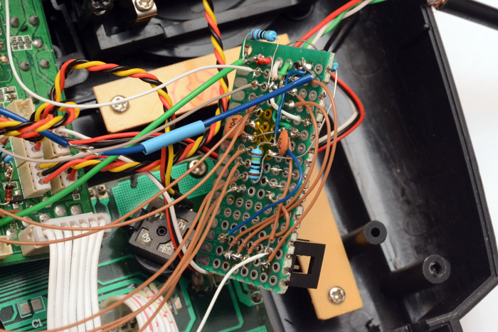
And the finished hardware:
Now to write the software. Usually I finish the software before the hardware is fully done, but in this case we're confidently leaving the software till last. The programming port on the protoboard means we can immediately test it in its final configuration. In fact, the software is very simple here:
- If USB voltage isn't present, go to sleep
- Load up the report descriptor for a USB joypad
- Loop indefinitely, filling out the report buffer with analog readings from the pins
I must admit that for the ATtiny85 USB projects, I'd for some reason thought it would be easier to use Atmel Studio to compile them. This caused me no end of hassle in terms of trying to import the USB library correctly, so after struggling through that the thought of switching to a different chip was daunting. But, by downloading WinAVR you immediately get the complete build environment as it would be on a linux system, and the makefiles provided by objective development work straight out of the box (except for one line about checking size, which I commented out). Setting it up with WinAVR was vastly less painful than using Atmel Studio.
With that, I'll stick the finished code up on github. I gave the controller a quick test flight on the simulator and all was dandy (except that the sticks are wired up inconsistently with respect to the previous controller, but that's totally irrelevant).
I suppose this is quite a boring project, as projects go, but it's nice to do things right. There's also still that satisfaction in being able to extensively modify consumer electronics without breaking it. Unlike software, there is no Edit>Undo, and unlike most hardware, there is almost no way to replace a part if you break it. And in this case, the equipment I'm modifying doesn't even belong to me. Currently, this is the closest I get to living on the edge!