
LED Matrix Earrings
20 Feb 2024Progress: Complete
I originally imagined the LED Industrial Piercing as a project specifically to make use of 0201 LEDs. In the end, they weren't even necessary. 0201 LEDs are just too small! Evidently, we needed to go deeper, so the purpose of this next project was to stick as many as possible of them onto the face of a stud earring.
Watch the following youtube video for an extensively narrated journey.
Continue reading this page for an in-depth explanation.
Design
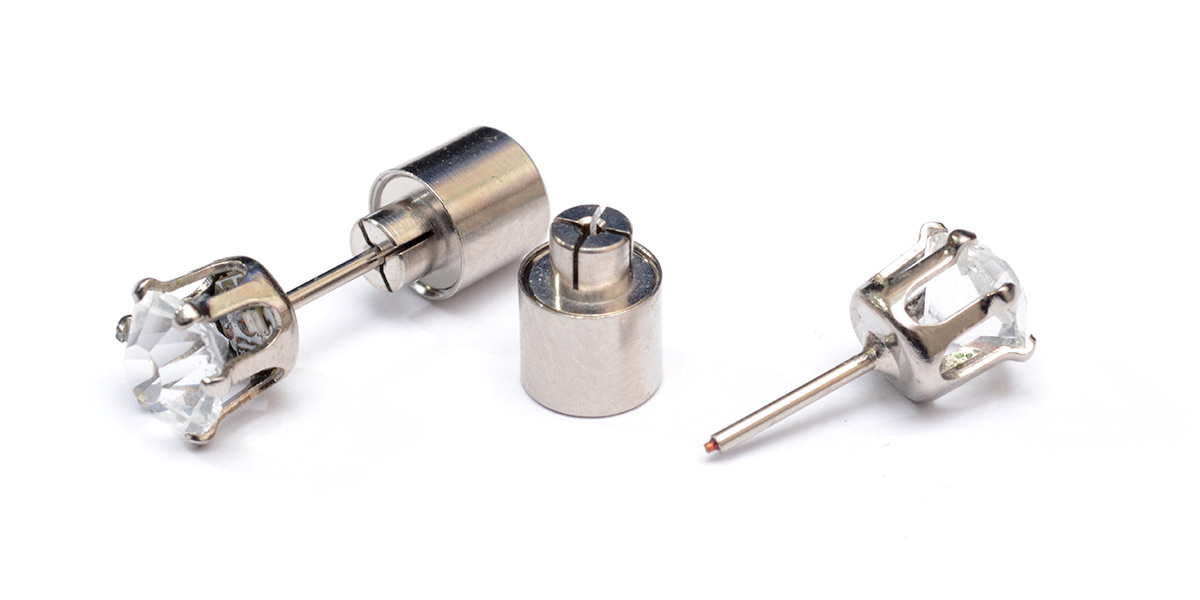
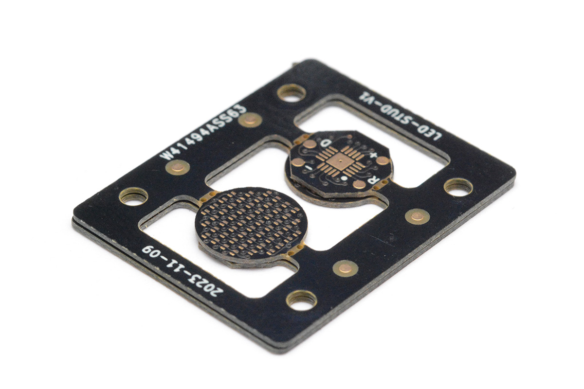
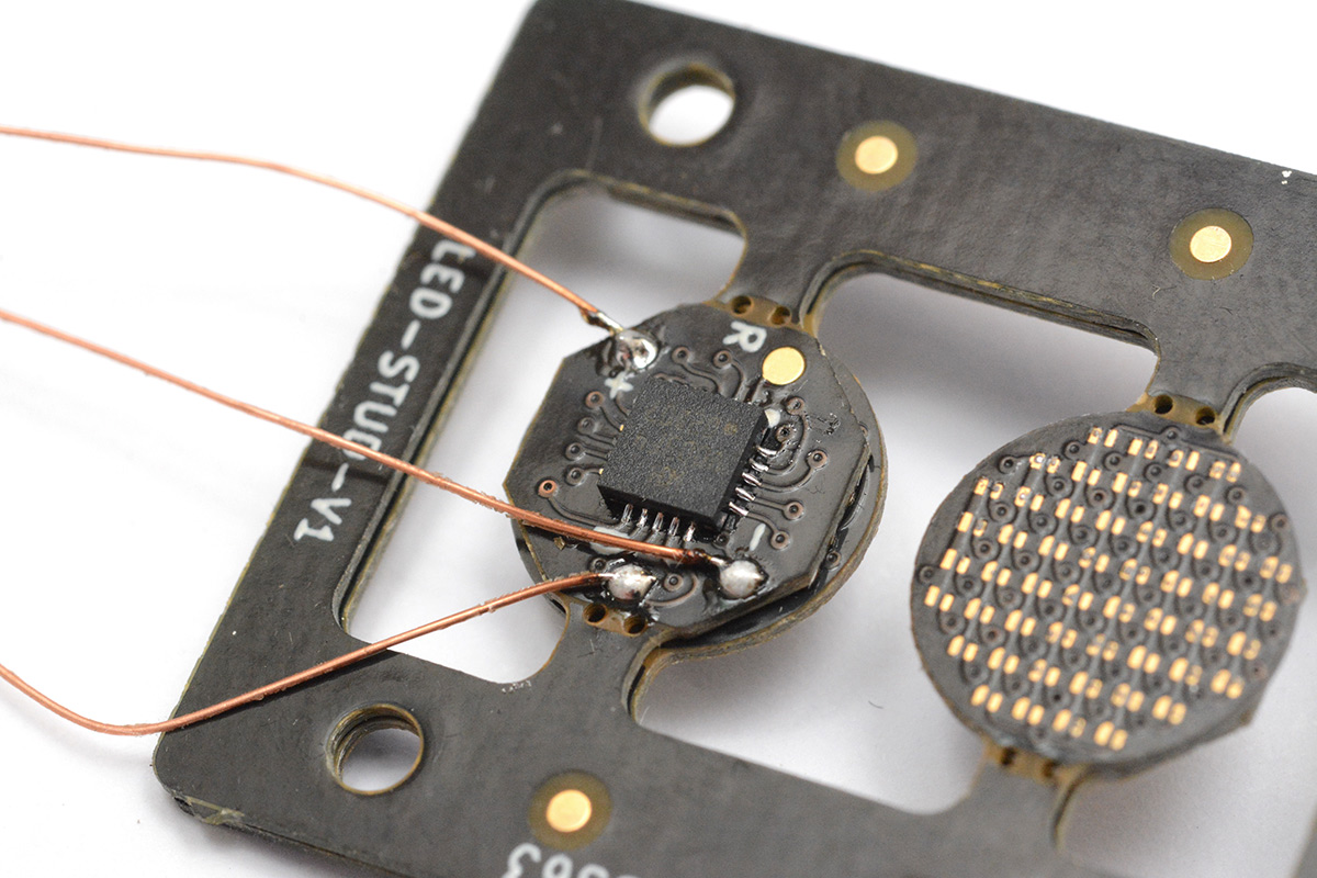
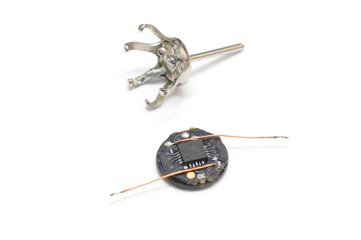
These off-the-shelf LED stud earrings are very cheap. They have a tiny machined battery holder for two LR521 cells. The idea was to replace the plastic gemstone and single LED with our own circuit board, re-using the metalwork.
Electrically, the circuit and firmware would be identical to the badge I recently created using a CH32V003. Read that page for the story behind it and an explanation of how it works.
![]()
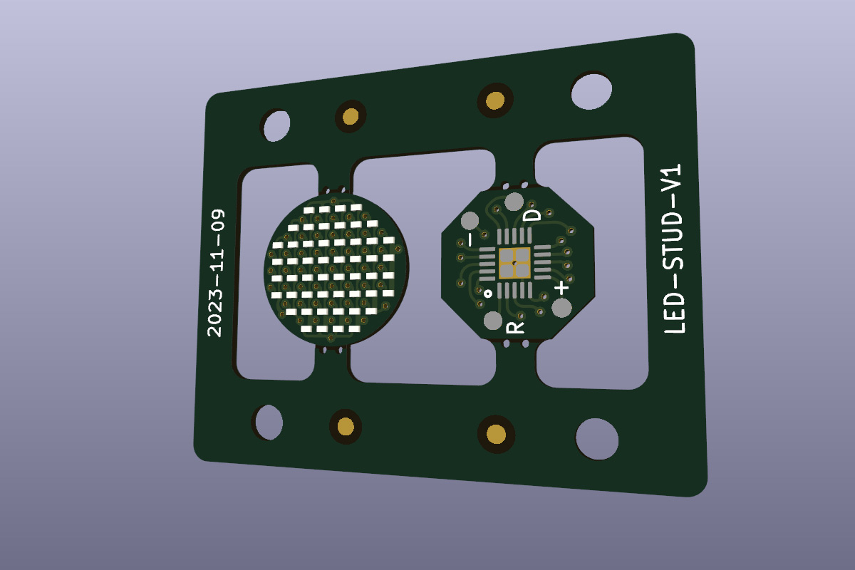
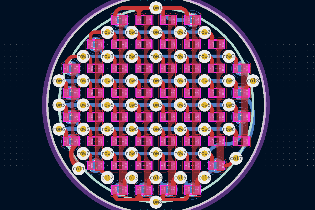
The challenge here is shrinking the design of the badge by a factor of 3 (or one-ninth the area) by shifting from an LED pitch of 3mm down to 1mm. We also insisted on not having a thick border around the board. This poses quite a challenge for routing the tracks.
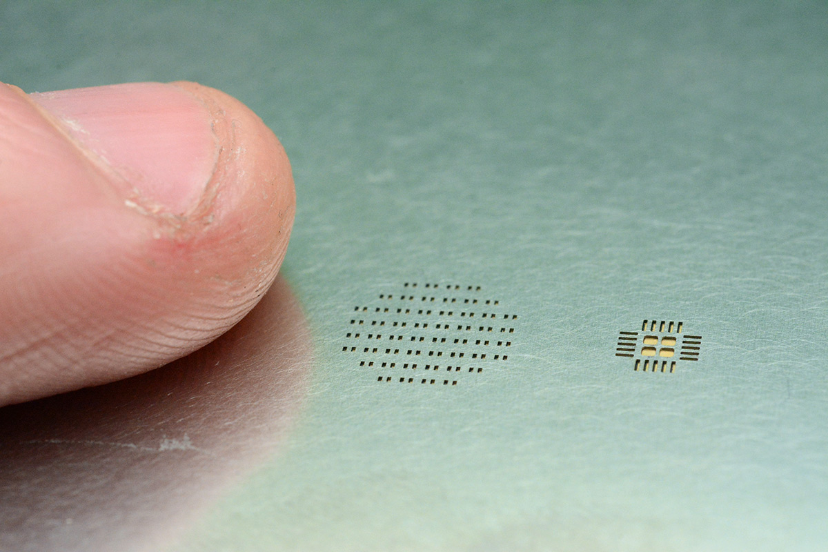
To give a sense of scale, here's three 0201 LEDs next to a regular surface mount LED:
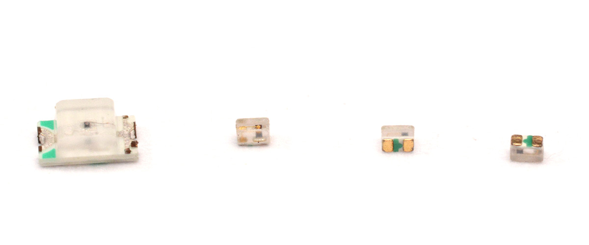
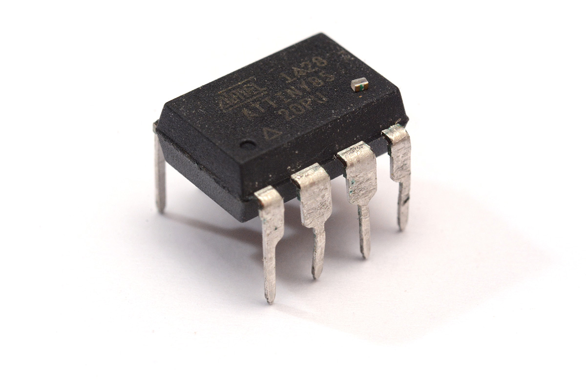
Or, to really put it in perspective, an 0201 LED on the back of an ATtiny85:
Homebrew blind and buried vias
It's possible to get multilayer boards made with so-called blind and/or buried vias. The limit is far, far beyond what we're working with here. The "redistribution layer" of BGA packages is normally built as a very small, high-density circuit board. These often have very fine pin pitches and use blind vias, via-in-pad, and so on. The point is we could easily order a circuit board to these tolerances – if we had the cash for it.A small batch of HDI boards starts at several hundred dollars, and the more complex the stackup the more the price goes up. I would very much like to keep this entire project under $50 total.
I decided to craft my own circuit board sandwich, two two-layer boards held together by an array of solder pads.
I wasn't sure if this was going to work. I put all the pads around around the perimeter, partly with the idea that I could inspect all the connections, of course that would mean removing the boards from the panel to do so, which I didn't want to do until the rest of the board is assembled. I suppose we could have started by fitting the components, and sandwiching the boards last, but that sounds like a recipe for disaster.
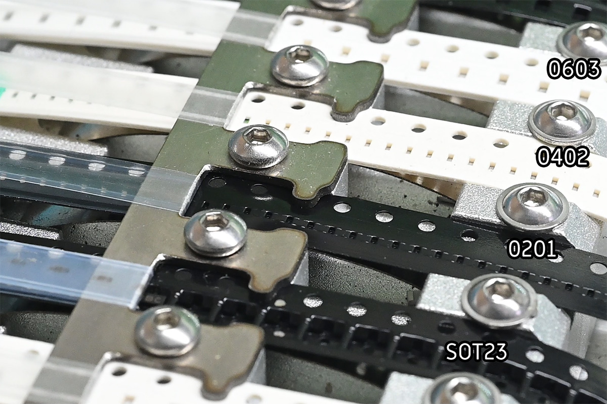
The drill diameter for the vias is 0.25mm, which puts us just into the second tier of board pricing (almost all of the cheapest PCB offers have minimum 0.3mm). It may have been possible to do a layout of 0201 LEDs within the cheapest tolerance, but I didn't want to risk it. Remember the distance from one LED to the next is 1mm. At this sort of scale, the copper thickness around a plated hole is noticeably uneven.
Solder sandwich
As usual, I combined postage with several other orders, which leads to a mini-christmas when they all arrive.
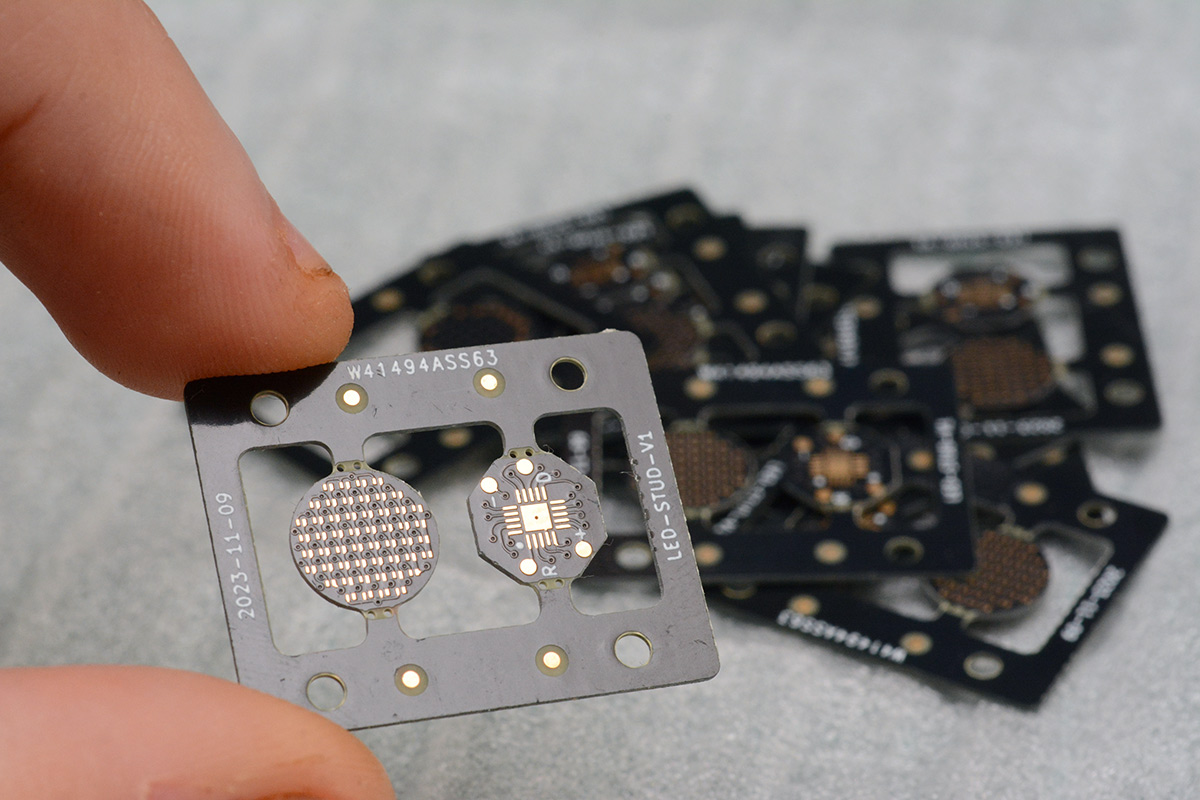
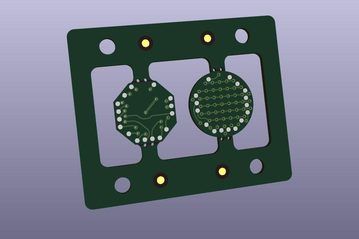
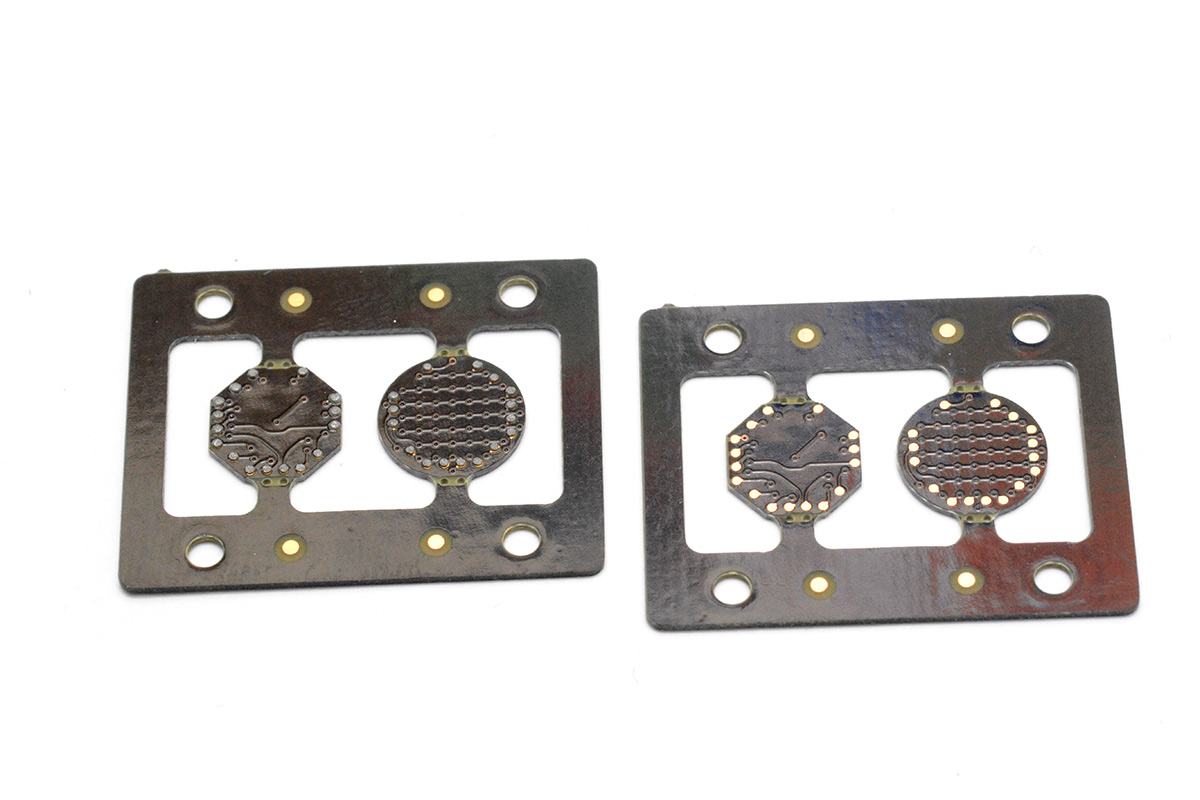
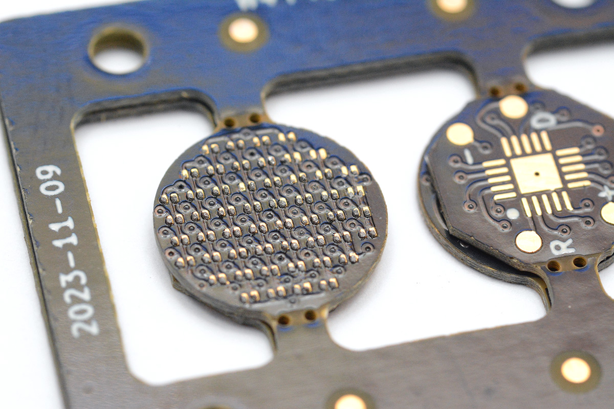
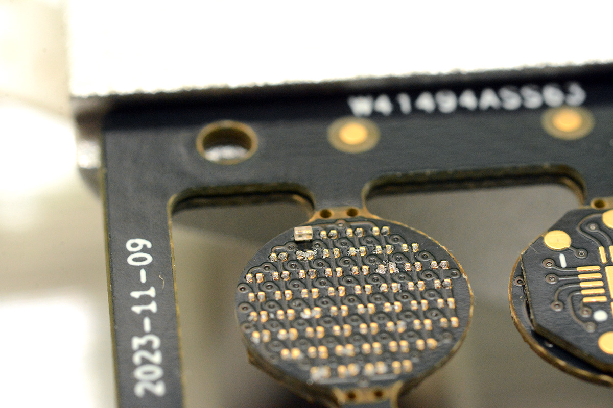
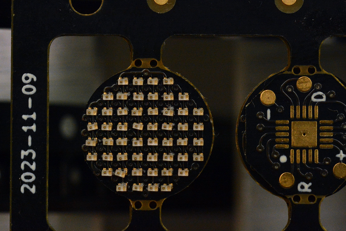
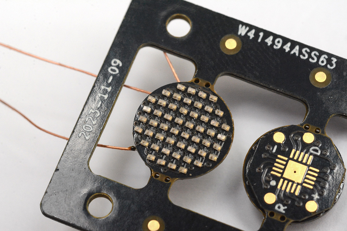
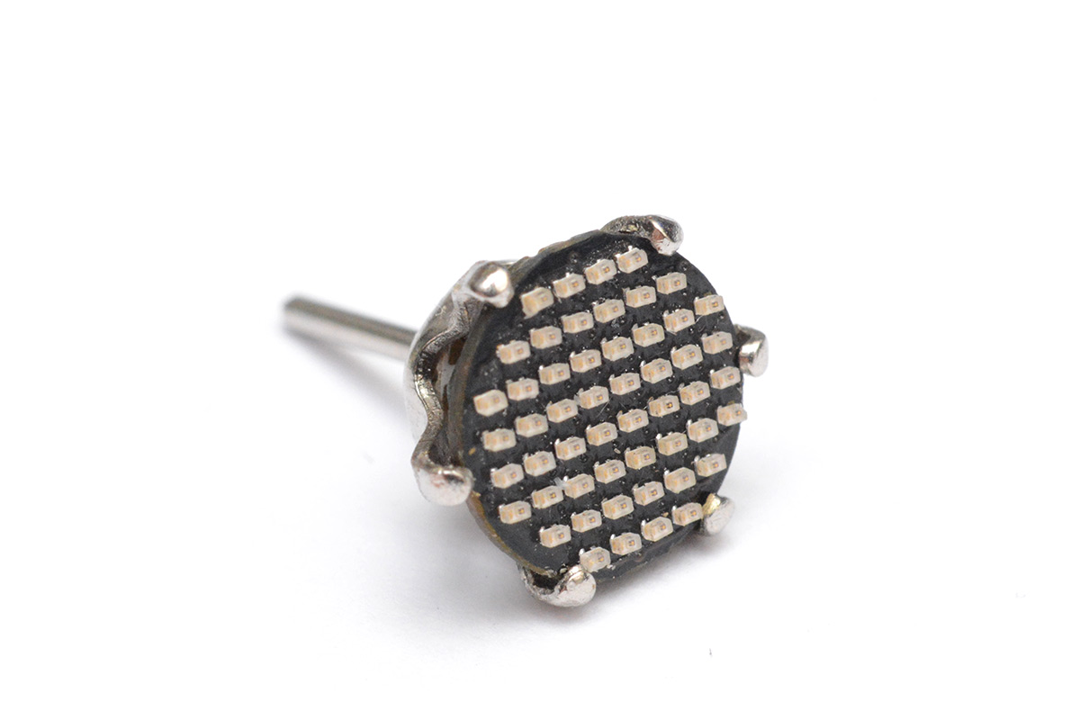
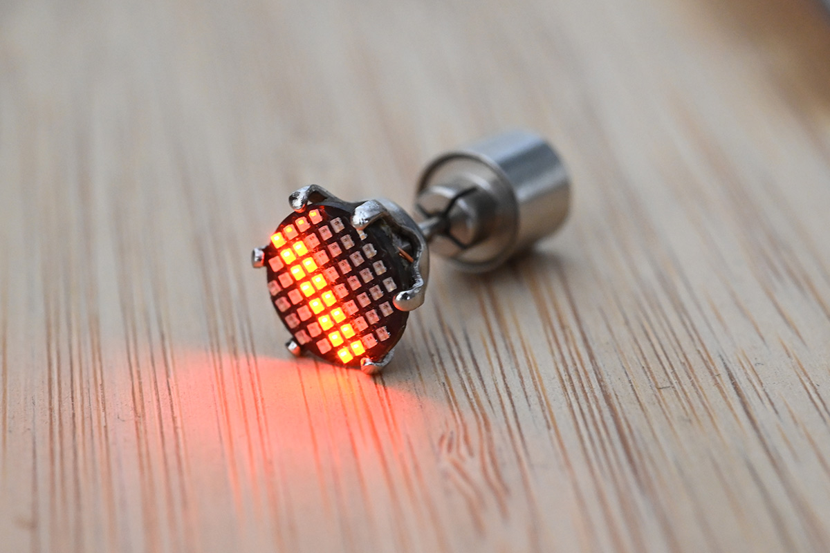
The main display is an 8x8 matrix at 1mm pitch. With the corners cut off to fit into the round profile, that adds up to 52 LEDs within a 9mm diameter circle. The panel top and bottom is 5mm wide. The whole panel is 23mm by 28.5mm.
I stencilled paste onto one of the boards, and sat an unpasted board on top of it. The symmetrical panel helps ensure perfect alignment.
The total board thickness is 0.6mm, so our sandwich ends up a little over 1.2mm. This was reflowed in a fairly uneventful way.
I probably should have used higher temperature solder for this step, as it would reduce the risk of these joints separating later on. On the other hand, I didn't want to risk messing this up, those pads are still quite small at 0.5mm diameter and it's not like I keep a whole range of solder pastes in stock. (They have a shelf life, and go off after a few months anyway.)
Paste paste paste
I ordered a steel stencil along with the boards. I fit about six other designs into it, but even ordering a stencil for one board is normally viable, they're unbelievably cheap for what they are.
My first mistake was not putting the fiducials on the stencil. Aligning the first board was easy enough, we could use the QFN pads to confirm it, but after cutting one board out of the panel, aligning the second board was very difficult.
My second mistake is possibly making the holes for the 0201 pads too small. I probably could have gotten away with a smidgen larger, which would have made the stencilling process less stressful.
The first attempt wasn't too shabby, most of those pads are perfect with just a few under-pasted. I wiped this off and tried again a few times, I feel like with exactly the right amount of pressure and speed with the squeegee it should be possible to get it perfect.
I didn't quite manage perfection, but got close enough to feel like moving onwards. I did clean the stencil at this point, but not sufficiently. The remaining residue would dry up and cause me to have a much less fun time when it came to the second earring.
Pick and place
Presuming the reader has already watched the video, or at least perused the previous projects of the badge and the volumetric display, it goes without saying that I planned to position the parts with the pick and place machine.0201 is well beyond the specified tolerance of it, so this was something of a gamble. It's not impossible to place 52 0201 LEDs by hand if it came to it, but I was really curious to see if I could do this, and if so, what further projects that opens up in future.
The machine came with a selection of vacuum nozzles, most of which are cylindrical, but the very smallest is this shape.
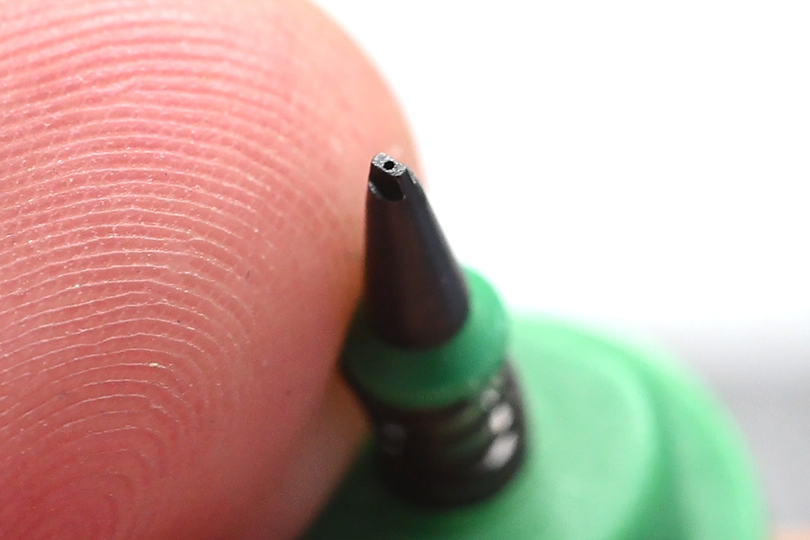
That oblong tip is a comparable size to the parts we're trying to pick up, so it wasn't clear if this would work, but in the end it didn't seem to have any problems in this aspect.
The construction of the machine appears to be little more than a glorified 3D printer, but evidently it's built to a much sturdier tolerance. Once I'd calibrated the position of the components, it placed the first one absolutely spot-on.
The problems I initially encountered were less about component placement and more about the tape misbehaving. I have the machine on a very sturdy desk, but it still shakes about as it operates. This means parts as small as an 0201 LED are likely to go flying if the protective film on the tape is pulled back. The holes in the tape are at a 4mm pitch, just like all the other tapes, and most parts, even quite small ones, are placed at a 4mm spacing. It's only when you get to 0402 and 0201 that parts are placed at a closer spacing than the holes in the tape. This poses something of a problem for the mechanism used to advance the tape: the head has a solenoid pin which it inserts into a hole and pulls it forwards. For tapes with a 2mm spacing, it needs to advance by half a step instead of a full one.
The machine is able to do this, but the key factor in getting it to pick parts reliably was to offset the position of where it picks up the part out of the tape. The zero position is almost 4mm away from the area where the film is peeled back, which offered far too much leeway for parts to bounce away.
I'll fast forward to the end of the first attempt.
All in all I was pretty impressed with that. There's an obvious systematic error, all of the parts are a little too low, but that's just my inaccurate calibration, the placement is very consistent with itself. A few of the parts are skewwhiff, it's not clear if they jumped as they were put down, or if there was an error in the vision system. Even a small rounding error in the OpenCV outline logic could lead to it placing the parts at a weird angle. Luckily it's trivial to push the odd part back into place.
After reflow, virtually all of them snapped into a perfect grid alignment.
The result is quite a bit more consistent than my second attempt on video, just because I did a much worse job of stencilling the paste that time.
Populating the back of the board was somewhat uneventful.
Uneventful, but not without suspense! It wasn't until this point we get to check if any of it works of course.
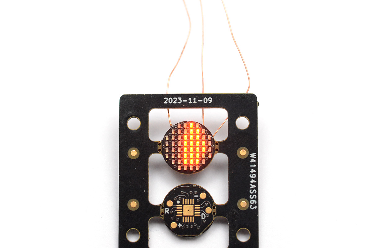
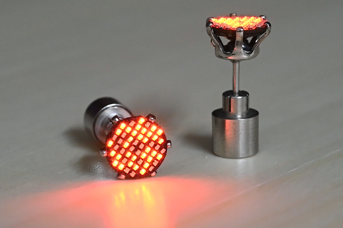
Sweet.
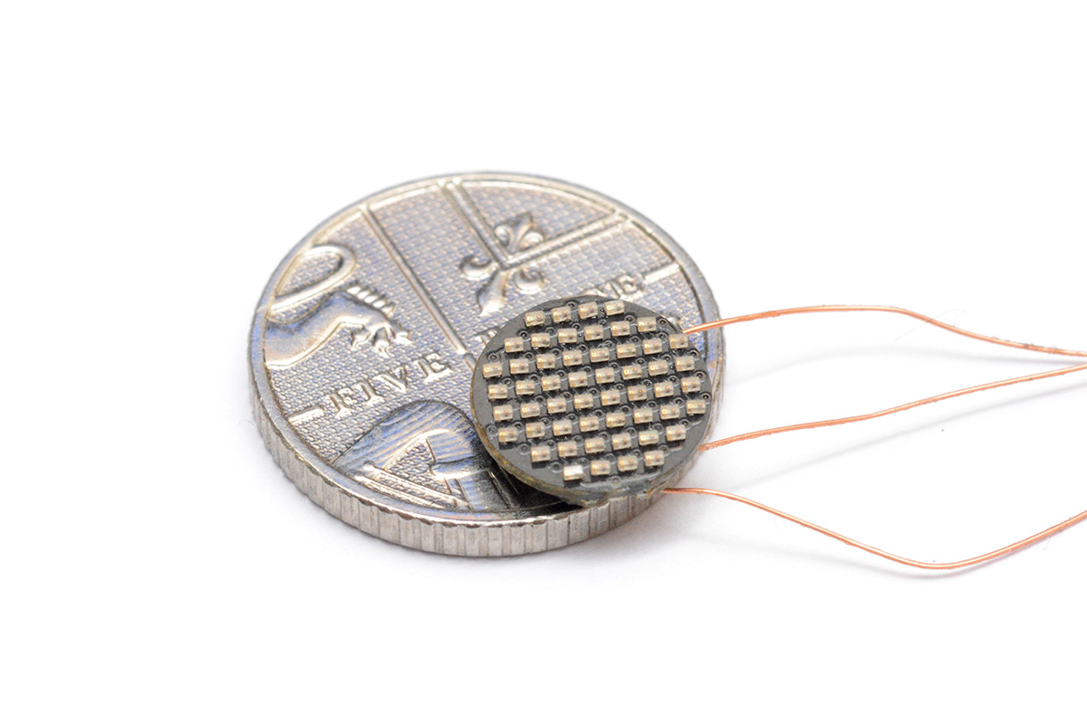
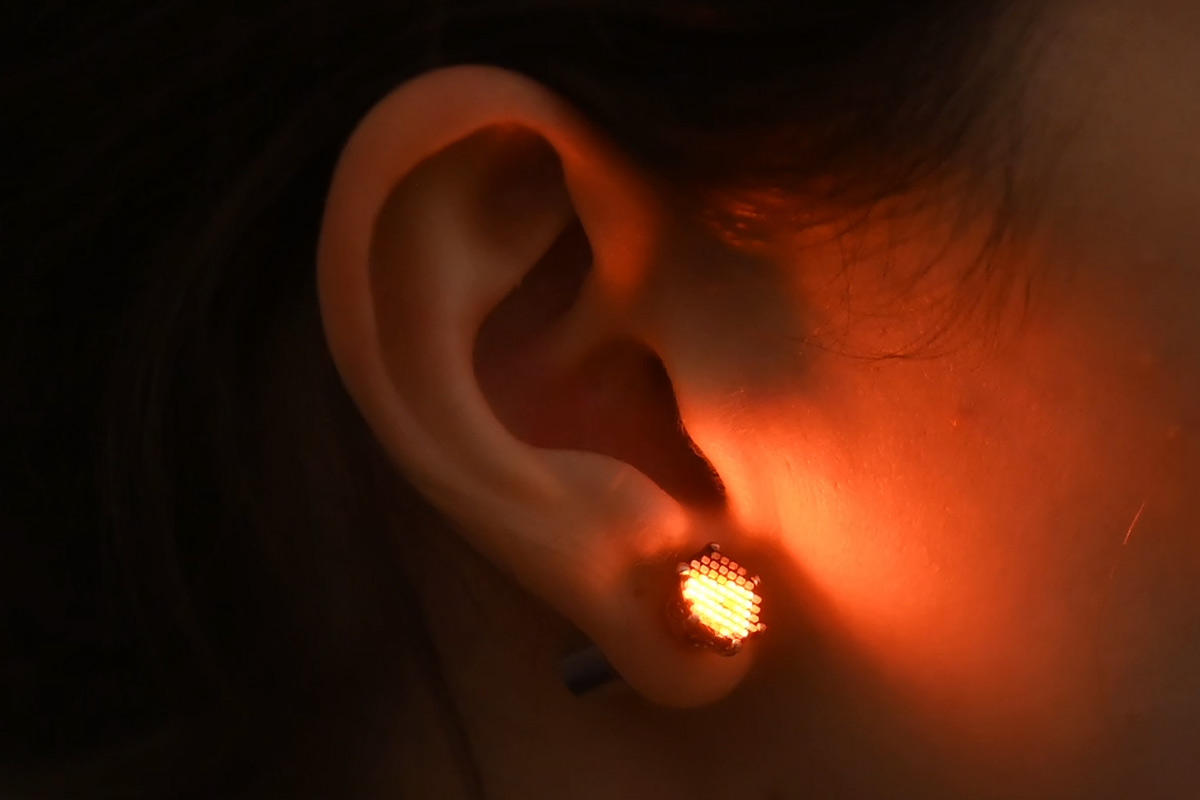
After chopping this out of the surrounding frame, we took a moment to do some vanity shots with a coin for scale.
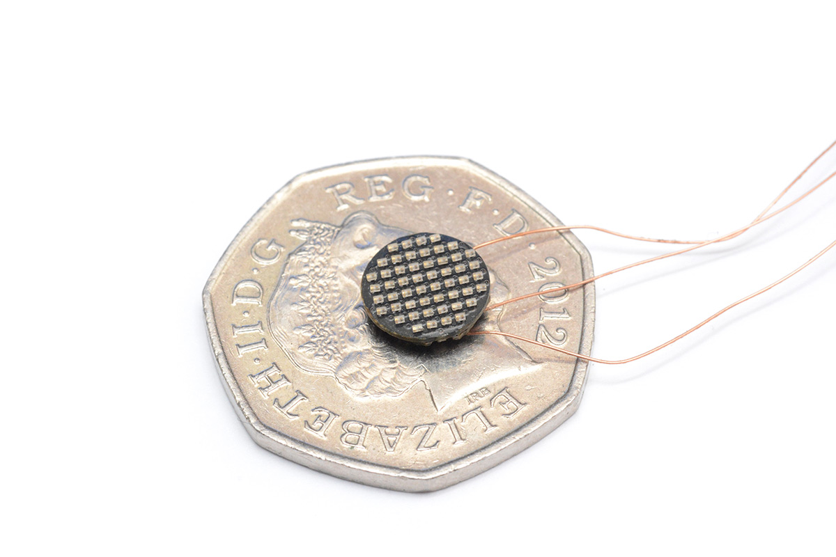
The 50p coin is of course a little large, so here's another shot on a 5p coin, much more appropriate.
Stud preparation
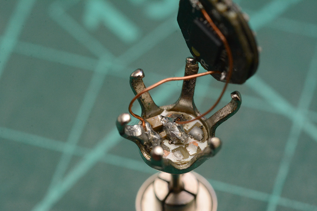
Under the plastic gemstone, the stud earring has a tiny circuit board with two components on it.
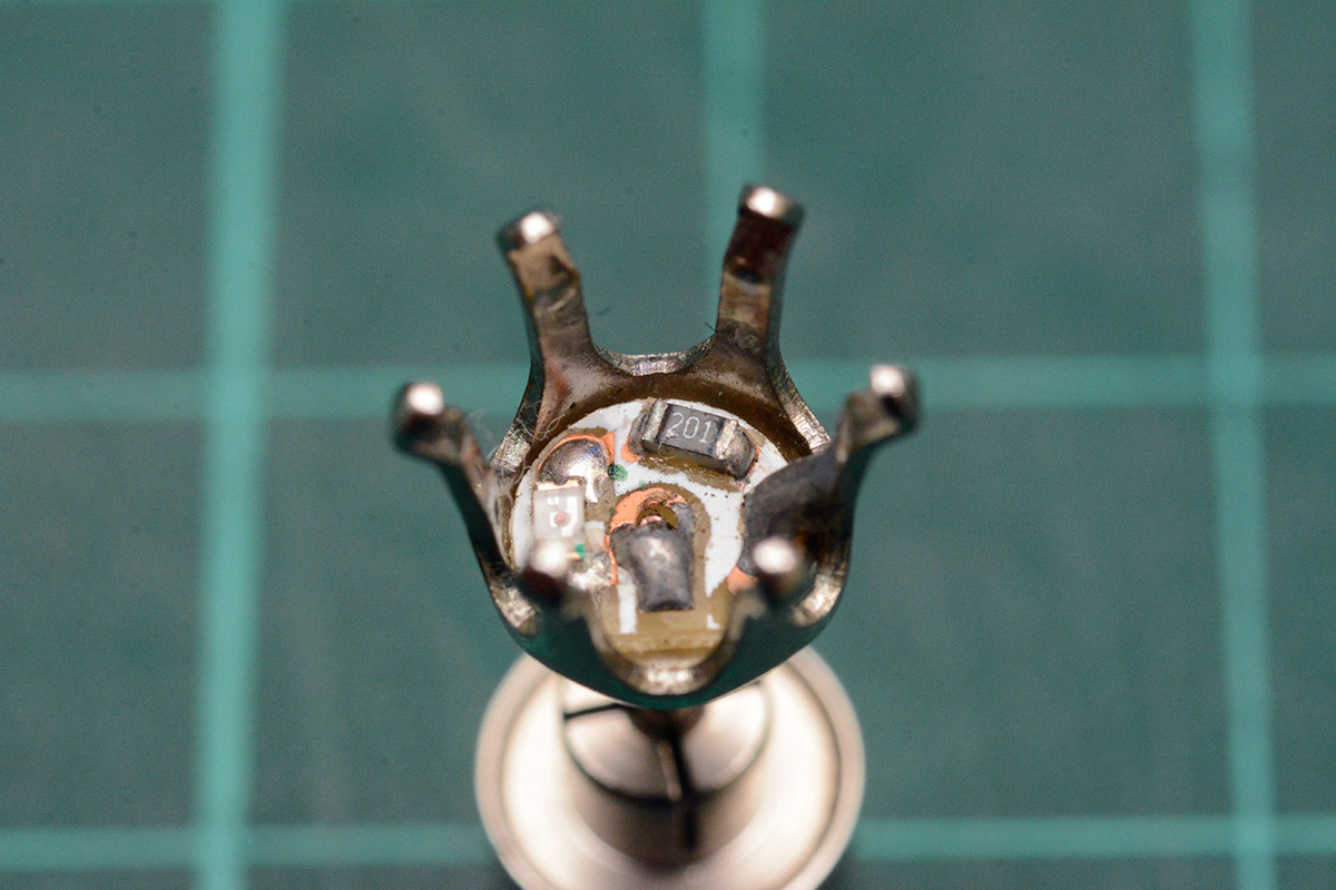
The case is the positive terminal of the battery. The negative terminal is a fine wire through the middle of the post. We just need to connect our circuit to these two points.
Rather short-sightedly, I soldered the connections in place and set the circuit without fully testing it. I was exceptionally careful with setting the prongs, which was silly as I soon had to undo this and modify things.
The power draw of my original firmware was far too high, it's dumb I didn't see it coming. The teeny battery can't cope with the current draw, the voltage drops and the CH32V003's brownout detector resets the chip. With some further digging into the datasheet it might be possible to disable the brownout detector. I'm more used to the ATtiny chips, many of which are happy to run down to 1.8V.
It is just about possible to reprogram the circuit with it set in place, I use a crocodile clip to connect the positive terminal, touch one wire to the end to make the ground connection, and then touch one more wire inside to make contact with the debug pin. However, doing this more than once is a right pain, so I opened up the earring again to do things properly.
While we're at it, adding some capacitors is bound to help.
That's a 22uF and a 0.1uF in parallel. Sometimes large-value, physically small ceramic capacitors have a high internal resistance so it can be helpful to combine multiple values in parallel like this.
I dropped the clock speed of the chip from 48MHz to 1.5MHz, and one of the things I found is that this affects the debugger connection. Ordinarily this is fine, there's a utility that lets you "unbrick" the chip by power cycling it and immediately connecting. This unfortunately necessitates debug control of the power supply, which is why it becomes very fiddly in our situation, and is what led to me trying to connect to the earring post with crocodile clips.
In the end I got the display into a state I was happy with, a duty cycle of about 0.25% and the reduced clock speed means the overall power draw is something like 8mA.
With that, we were able to call it done, and begin work on the second one, which had the added fun of a video camera in the way of everything.
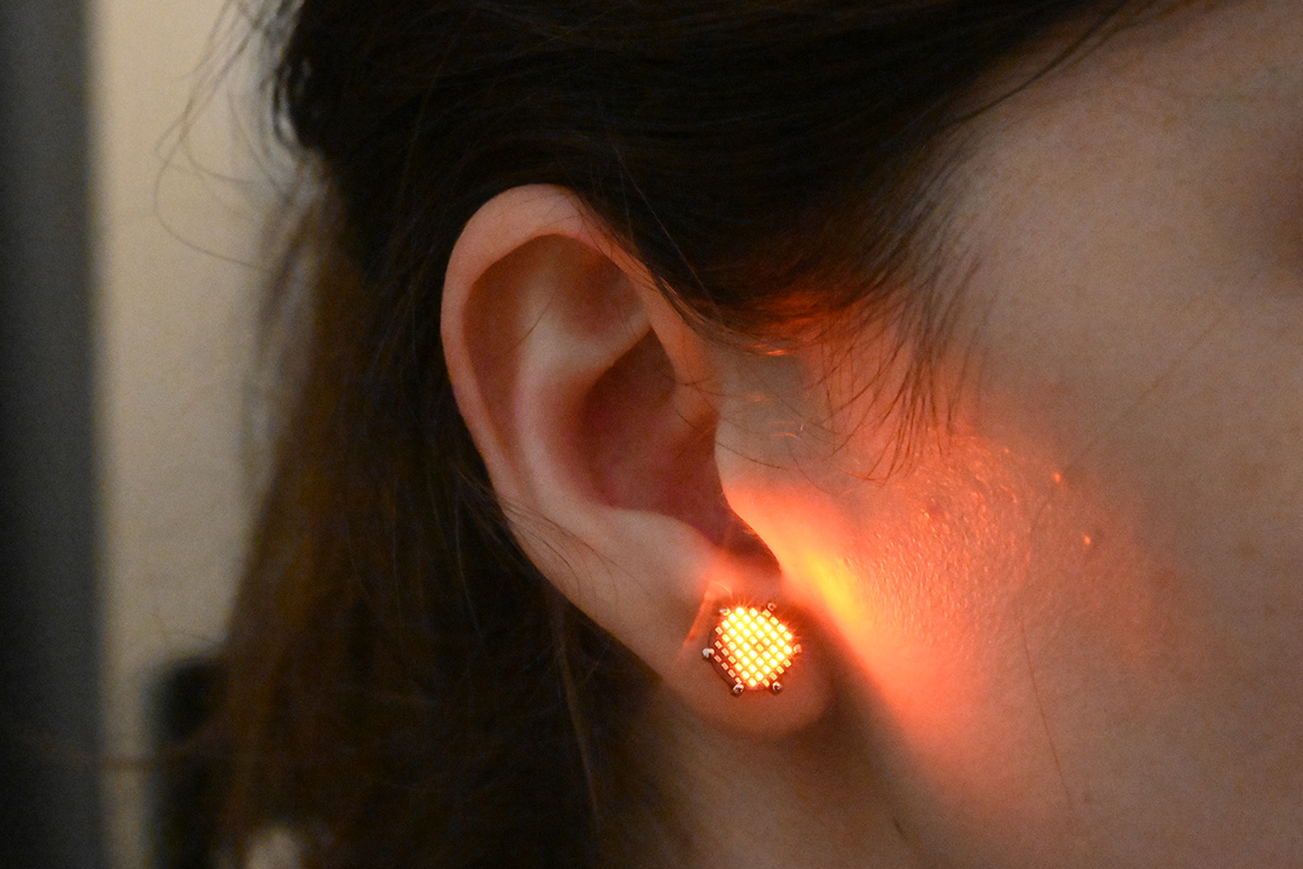
Vanity shots
You may have clocked a certain amount of self-doubt I expressed as I came to set the circuit. It's an impressive electronics project, but is it an earring anyone would want to wear? To be fair, it's not like that's stopped me in the past from building utterly tasteless earrings that no one would be seen dead with.
But my friend seemed quite keen to try on more glowy glowy accessories. I suspect she secretly enjoyed being an ear model.
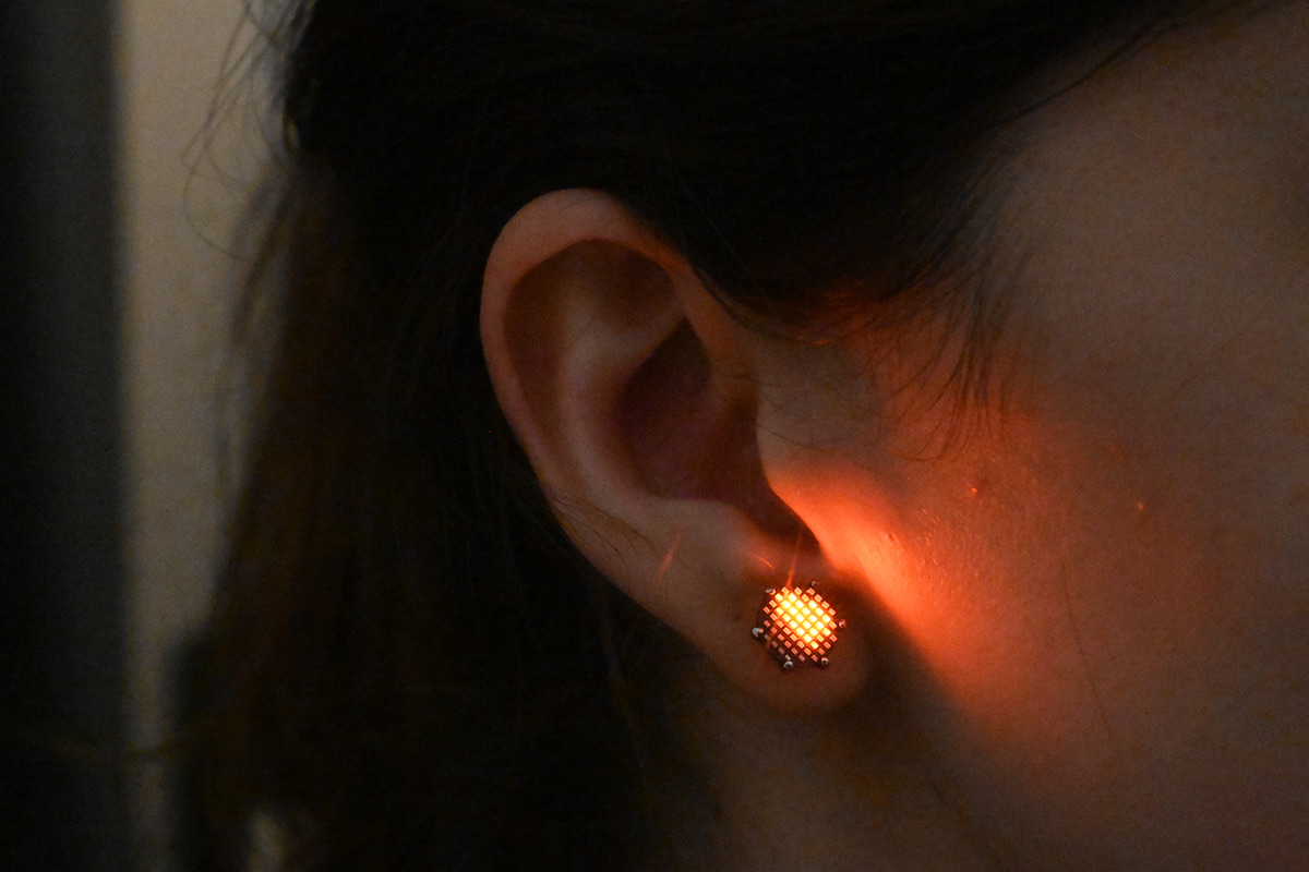
One idea I'd meant to try with the industrial piercing is combining a long exposure with flash, to try and get a still image with LED trails.
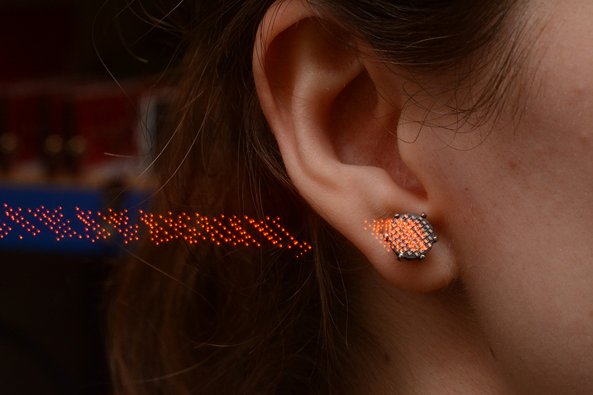
This led to a somewhat inevitable conclusion. Believe it or not, it was her idea.

The source code for this project is identical to the badge, and is available on git.mitxela.com and github.