
Games Console Circuit
22 Dec 2018Progress: Complete
* * *
I originally built this on a breadboard. At one point I was planning to produce a PCB, but that petered out and I figured, to hell with it, I'll just make it all on protoboard.
There is an Eagle schematic, but even looking at it now I can see a mistake, one output of each DAC is supposed to be tied to ground. They're just meant to be as the datasheet suggests. Here are some screenshots.
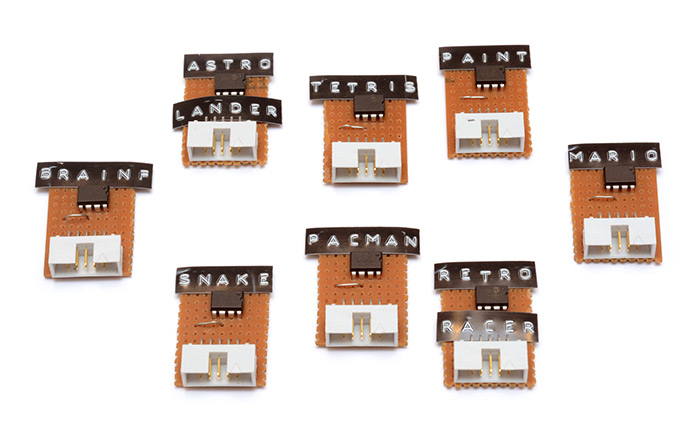
and the cartridges were pretty simple:
So, I ask you to join me on this adventure, as we assemble Mark II of the Games Console. Begin!
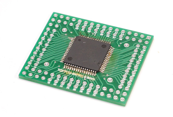
We start with the processor of course. I didn't think my soldering skills were quite up to ELM ChaN's extreme prototyping techniques just yet, so I got these nifty little TQFP breakout boards. And so the build began, with plenty of flux.
What's the bare minimum you need to wire up to get an ATmega128 working? Vcc, Gnd and the AVcc too, pull the reset line high and a crystal with the right caps probably won't hurt. And we need to wire up an ISP cable, to see if it is working at all.
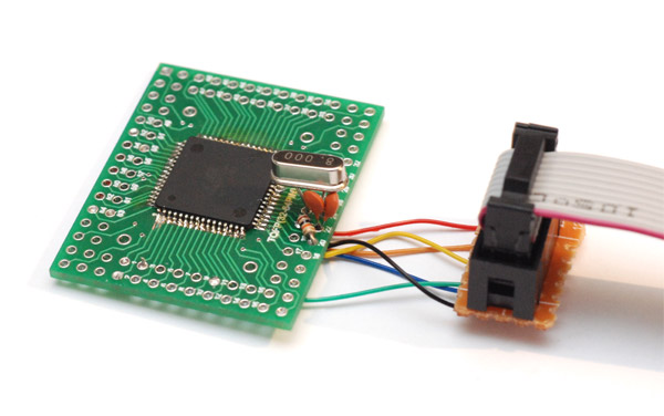
It turns out you're not supposed to wire the PEN* pin (program enable) to anything. Just leave it floating. This took a while for me to realise. Soon after, the chip seemed to be working fine.
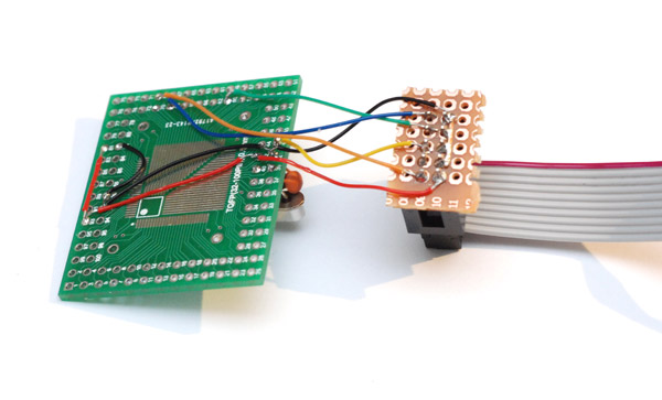
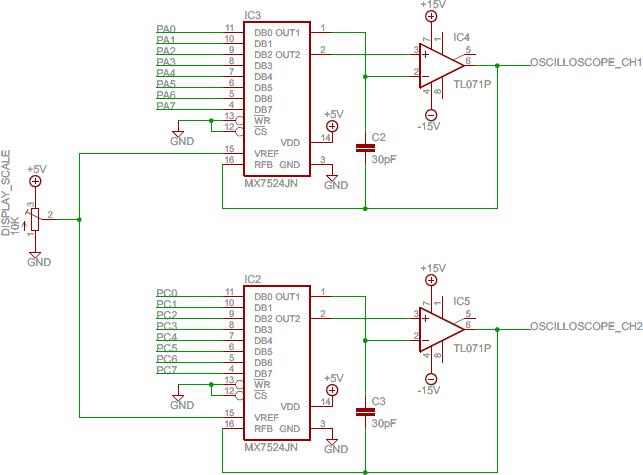
Better jump right in then. Starting with the vector video hardware. This is a pair of digital-to-analog converters and associated op-amps. The op-amps are 071s to be true to the original design (actually it's a single 072 chip which is a dual 071) even though this was something I said I'd change in the next version – they're easily the bottleneck of the design with a slew rate of 13V/μs. But I want this build to be true to the original. Two 8-bit parallel data lines go from the ATmega to the video board, which is upside-down in this shot. It's just the 7524 DACs, the op-amps and a trimpot for the reference voltage. This corresponds to the display scale, and is used to balance the slew rate / size of unwanted artefacts in the picture. More capacitors would be added later.
I really really considered rewiring this. But I wanted it to be true. Hmm. You see the op-amps are wired as inverting amplifiers and produce a negative voltage output. In the original, by the time I'd realised this I'd made several games already, even though it meant the origin had to be in the top right corner – a little annoying. But the real issue is that this time I didn't have a proper power supply with the +/- 15V rails. I didn't want to add more op-amps, that'd mean a worse slew rate, but it may have been possible to use them as summing amplifiers in their current configuration so that there wasn't such a heavy DC offset. But the main problem is providing them with a negative voltage. I want the final product to be simple and run from 5V. There are rail-to-rail op-amps I could use, still this would need rewiring though...
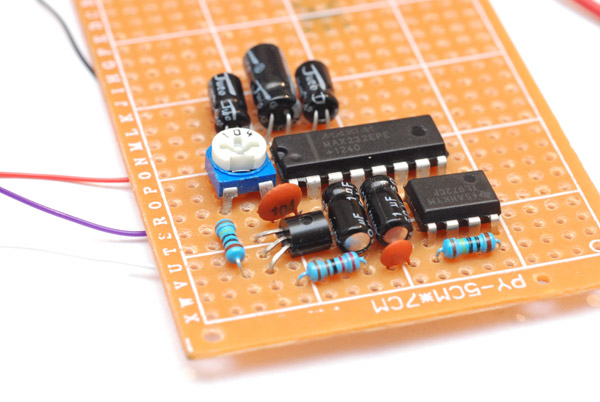
I figured they only need a wee bit of power, so we can cheat and use a MAX232 chip to generate the needed voltage. This is a level converter for RS232 signals. Incidentally, I doubt my Chinese part is actually made by Maxim, 'max232' has become a sort of generic part number. The chip has onboard a voltage doubler and a voltage inverter, so hopefully we'd get a +10V and a -10V from a 5V input. You provide the external caps for the circuit. It says in the datasheet you can draw a small amount of current from the pins.
Well, my chip was struggling to get to +/- 7V without any load applied. I had a couple of them and both of the chips had a strange problem where something, I never figured out what, would trigger them into some failure mode where they'd stop inverting voltages and start getting really really hot. The smell they gave off was a giveaway. But after cooling, everything was A-OK and no hint of what caused it.
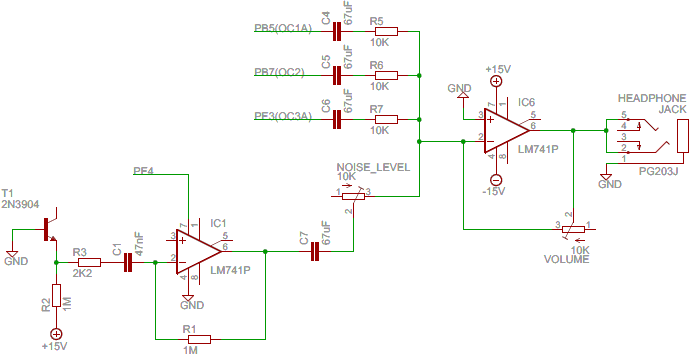
Oh, another reason we need special voltages – the noise generating circuit for the audio. It needs at least 12V, preferably more.
The problem with folding capacitors flat to the board, is as soon as you've done it once, you have to do it for all capacitors, or it wasn't worth it to begin with. Space is at a premium in my planned enclosure. Yes, I am the kind of person who files down the legs of a trimpot to give it a lower profile.
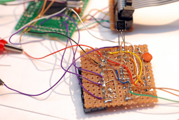
In the photo above, the big chip is the max232 and the small chip is another 072 dual op-amp, ready for the audio. Yes... another deviation from the script. Originally I had a 741 as a summing amplifier for the audio, and another, totally separate op-amp for the noise generating circuit. The power rails of the noise amp were ground and a lead from the ATmega, that is, the processor could turn the op-amp on and off by cutting the power to it. This used it both as an amplifier and an analogue switch. Is it allowed? No idea, but it worked. But this time, as I test-assembled the parts, I had the marvellous brainwave of saving space using another dual op amp and switching the power to the transistor that actually produced the noise. As I mentioned, this needs more than 12V, but with one leg to the negative from the max232, the other leg could go to the ATmega and if it's high it'd be more than 12V, and if it's low it'd be less and the noise would stop.
That was the idea anyway. When I soldered it together it no longer worked. Instead of a nice burst of noise, we were getting horrible clicks. Yikes.
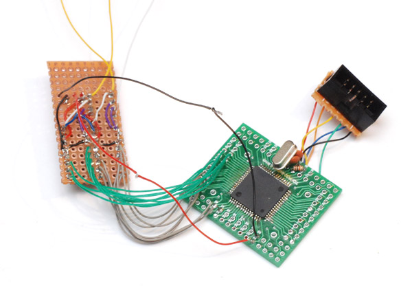
The pictures are a little out of sync with the narrative here. I don't know why I took so many of the power supply/audio board and so few of the video board. Maybe because the video board went through nowhere near as many modifications and rewirings.
The trimpot here is for the noise level in comparison to the square wave audio level. Even when I got it working, it was much quieter than expected. Maybe because I used a 2n2222 instead of a 2n3904. They're supposed to be identical but have different power ratings. I didn't actually measure the Hfe value before soldering it in, but I did find going through the rest of the bag that it varied wildly from transistor to transistor, even those from the same batch.
There's probably a good chunk of a farad on this board.
A number of modifications later, and I finally got the noise working, this time with the transistor permanently under breakdown voltage, and the audio signal being switched by a mosfet. I do like a good mosfet. It's a 2n7000. Great chip, the 2n7000. Sensitive though, very easy to blow.
You can just see it sticking up there as I finally had a working audio board. Then I moved it into a more permanent place.
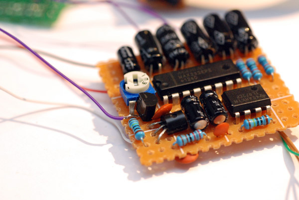
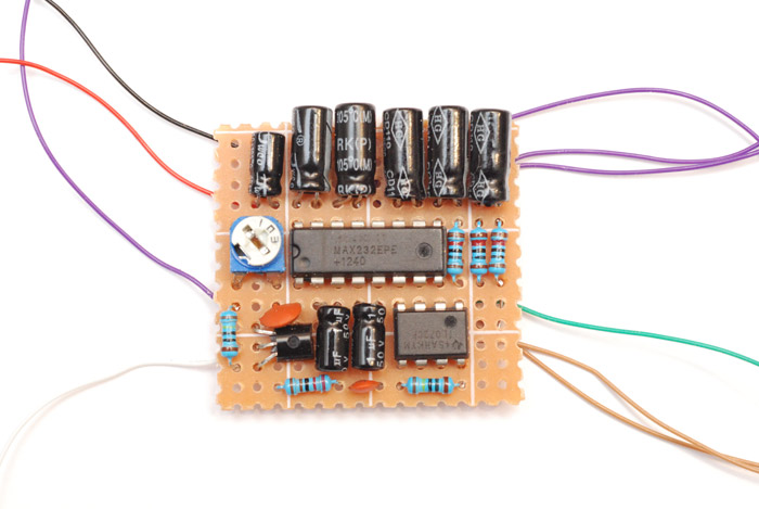
It snuggles in nicely (although sadly not folded flat) into one of the few spaces left. More capacitors added in several places, but don't worry, we're nowhere near done. There were tons more capacitors to add.
The final circuit of this version of the audio was something more like this:
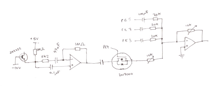
(Disclaimer: I drew that just now from memory, not when I actually built it)
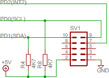
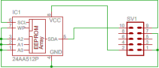
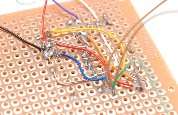
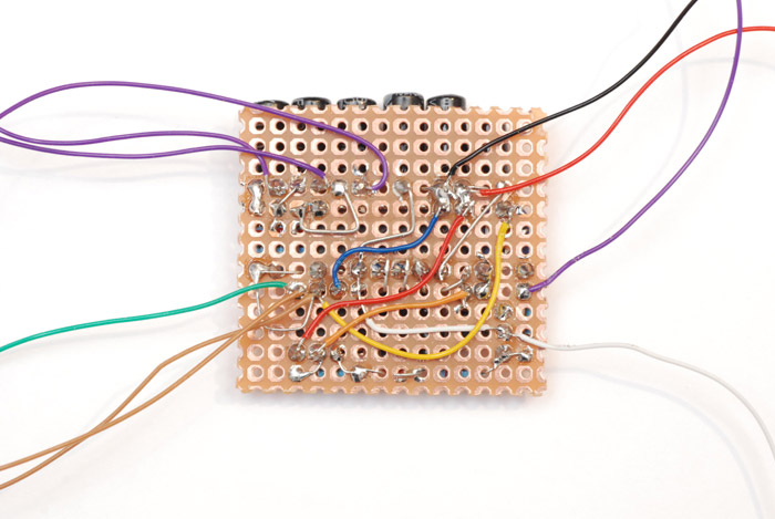
With that out of the way (or so I thought) it's back to the main board. The cartridges are just an I2C bus and power and ground. Since I'd already built and programmed the cartridges back at the time, it seemed silly not to reuse them. That meant reusing the connector though, one of those IDC ribbon cables. Well, wiring that to the board is straight forward, just a couple of pullup resistors. The challenge there will be mounting it to the case.
And what else? The controllers of course. These go to the SPI port. You can connect to a NES controller very reliably by poking jumper wires into the connector. That's what I did the first time. Someone suggested that for the final thing I should lop the connector off and solder straight to it. Sacrilege! You used to be able to buy NES and SNES controller connectors, but I couldn't find any now. What I did find were controller extension cables, which come with both male and female inline controller connectors. These would do nicely.
With the bulk of the soldering done (or so I thought), the testing began. Of course the ISP connector was only used once, to write the bootloader to it, and from then on all I had to do was plug the cartridges in. But no matter what I tried, I couldn't get the controllers working. One of the worries is that the ATmega itself may have been faulty, it did after all look like a knock-off considering how poorly the logo was etched. Maybe the SPI port was damaged? But for one of the games, Retro Racer, I'd bit-banged the controller communication and even that didn't work. I shall spare the reader the next several hours of investigation.
The problem turned out to be a faulty solder joint (shock horror, how could it be??) but I'd missed it because it was very subtle. After originally soldering the ATmega, I'd gone over every connection with a continuity tester. But by touching the offending pin with the probe, that pressed it into contact with the pad and it gave a good reading. How did this happen? Almost all of the joints were perfect, since I soldered them most carefully. But to begin, I'd tacked the chip in place by one corner. (In addition, I forgot to mention the chip arrived with most of the pins bent completely all over the place. But it was incredibly cheap.) To tack it I'd tinned that corner of the board first. And the way it had joined, the pin adjacent to the tacking pin, was left slightly lifted up. In future, the tacking shall be done with glue.
The real thing that kept me from finding it is that it was so close to the connection and with no internal pull-up enabled. This meant the signal was getting through by capacitive coupling but just giving erratic readings.
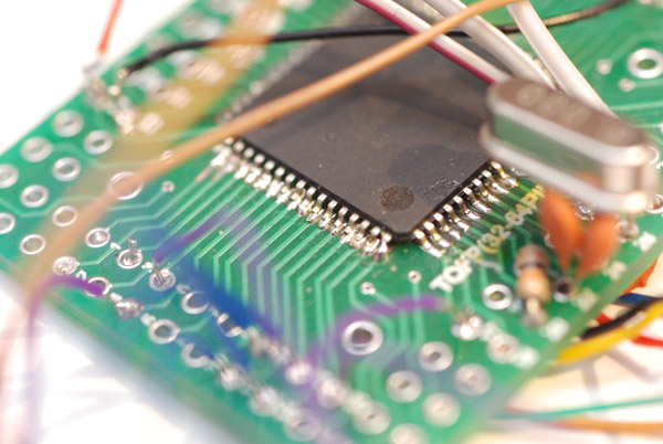
In that photo, the trouble was on the left, and it's been resoldered. However, it is now far uglier than the beautiful joints on the right.
This next photo is from eariler in the build, but it's an important one – the first time I fired it up and saw my beautiful pac-man ghosts again. You may think, from all the high quality photos I put up, that I live and work in a perfectly white environment. As can be seen in this picture, it's actually just a white piece of paper on my desk. The secret is out!
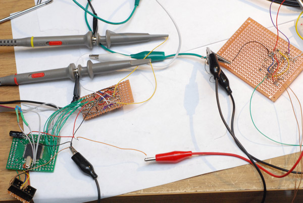
Using probes like that obviously isn't viable for the final thing. I needed to decide on a video cable. I'd already invested in phono-to-BNC connectors a while back, for funky music visalization times. Would these have the bandwidth for it? A phono cable probably wouldn't be all that great. Talking about distortion and such, there was plenty even with the scope probes. In fact it was almost unbearable, and the next few hours were spent cleaning up the analogue signal path.
This mostly means adding capacitors everywhere – little 0.1μF ceramics and big electrolytics all over. For filtering and for reservoiring. Generally, more capacitance was better. The main place that capacitance value is really critical is in the feedback for the DACs, where we feed a tiny amount of the high frequencies back into the input to prevent ringing. I worked my way through the values and watched how the step response changed, I think the final value was about 18pF.
Then, obviously to my delight, I found that the electrolytics on the audio/power supply board weren't enough and I had to desolder them and increase their value. This had a great improvement on the image, mostly the reservoir caps for the voltage inverter which I upped to 10μF or more (it only suggests between 0.1 and 1 in the datasheet). I should note that to try and reduce the load on the max232 I ran all the op-amps from only the negative rail, and connected their positives to the incoming 5V. I don't know if this made any difference. Hopefully, the scope probe / speaker connection won't be drawing that much current anyway.
Eventually I had a rock-steady image output. And I mean it, it's much better than I ever got in the original, and that had a "proper" power supply, like. Cool.
So what about the cartridges? Oh, but I'd already built these last year. Did I mention I got an embossing label maker? Well, I got an embossing label maker. Just to do these cartridges.
That about wraps it up for the hardcore soldering, onwards now, to build the enclosure.