
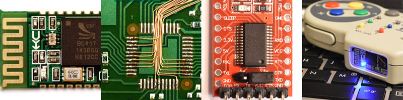
Bluetooth HID gamepad using HC-05 module
31 Jul 2016Progress: Complete
This project draws hugely on the work of other people. Part one explains how to load an HC-05 module with the firmware from the RN-42 without the need for a parallel port programmer. Part two builds an example wireless gamepad with the result.
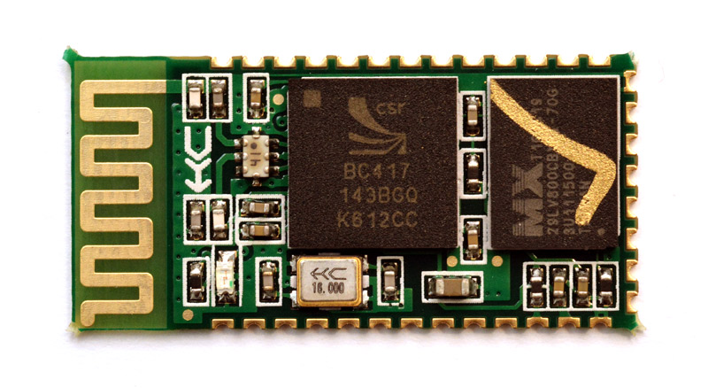
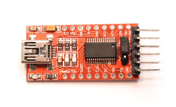
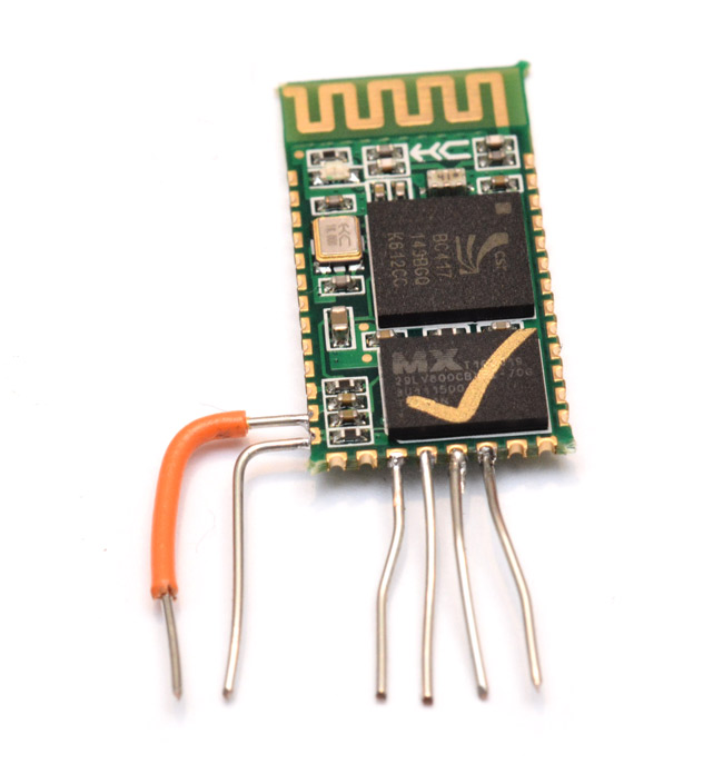
The HC-05 module is a bluetooth serial adapter and this one cost me £2.03:
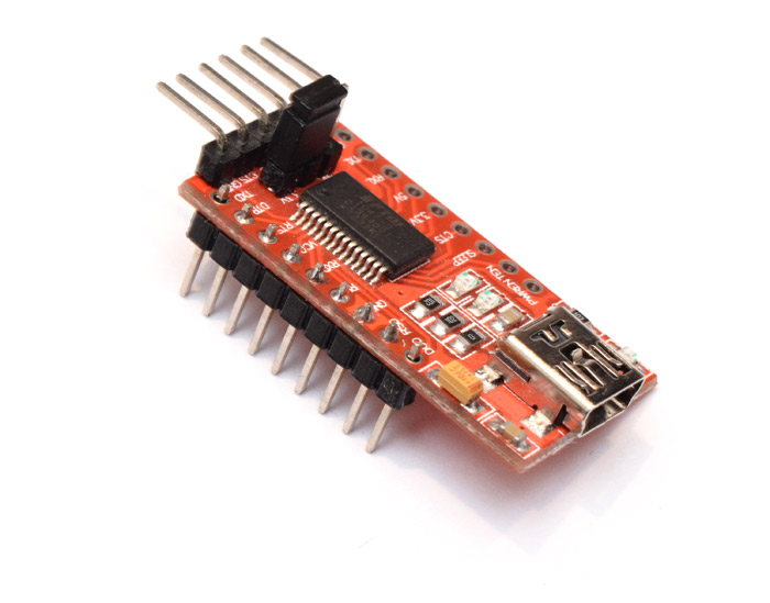
Here's a picture from the internet of an RN-42 module, a far more advanced bluetooth module, which costs over £20:
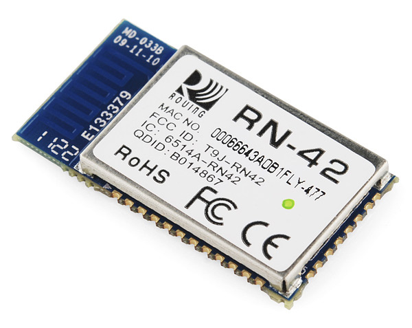
The thing is, under that shielding, the RN-42 uses virtually identical hardware to the HC-05, and its main chip (the CSR BC417) is the same. What makes the RN-42 more feature filled, and thus more expensive, is the software it's running. And software can be pirated.
From what I can make out the first person to realize this (or at least the first to write on the internet about it) was Robin Gross, whose site is called Byron's Blog. The process involves building an LPT (parallel port) adapter which then bitbangs the SPI communication to the chip. Inconvenient!
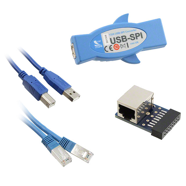
It seems that all the copycat tutorials on doing this also need a parallel port adapter. Parallel ports are soooo last millennium. Even CSR don't use them anymore. There is an official CSR USB-SPI programmer, and it costs OVER TWO HUNDRED POUNDS.
But there is a way to rewrite the firmware using just an ordinary FTDI serial adapter. Like this one:
This is possible entirely due to this project on github and its various contributors.
The first step is to acquire the BlueFlash software from CSR. Note: the SDK and other development tools are not free and not available to the public, but the BlueFlash software suite, which can reprogram chips and change their settings, is free. But you have to register with CSR to get it.
The download page for their software is https://www.csrsupport.com/PCSW and if you visit that link you'll be prompted to register. Once they've approved you, you should be able to download a copy of BlueSuite – I got BlueSuite v2.6.2 as it was the latest version.
There are other links, and only part of the category tree is visible. Every PDF you download has your username and email watermarked across each page, and a warning not to redistribute it. Yet it's freely available, for a given value of free.
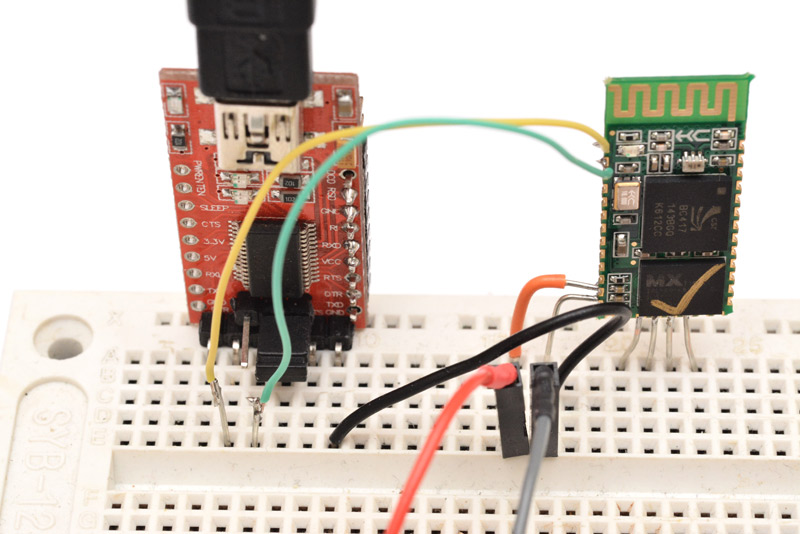
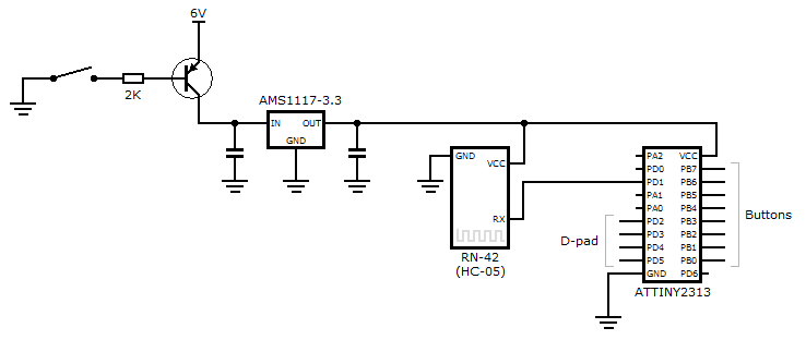
The plan is to bitbang the SPI protocol using the auxiliary pins of the FTDI board as GPIO. We'll need four pins to do this, DTR, RTS, RI, and DSR. These are available on the edge of my breakout board, so I added another row of header pins.
Note that DSR is labelled on the silkscreen of that board as RSD. A sure sign of quality. Thankfully, if it is a counterfeit board, it has not been bricked (FTDI have a history of pushing driver updates that brick knockoff chips).
Unfortunately – this is all on windows, by the way – unfortunately the windows COM port mechanism is not sufficient for our needs, and we will have to (temporarily) replace the FTDI driver with a libusb driver for lower level access to the chip. As described on lorf's github page, there is a convenient tool for doing this called Zadig. Download and run this executable, plug in your FTDI cable and click options > list all devices.
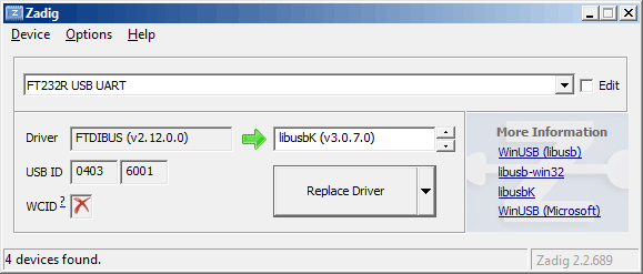
Select your FTDI device and then scroll through the replacement drivers to select libusbK, then hit replace driver. (Note: Make sure you really did select the FTDI device, and not, for instance, your USB mouse, as this will cause it to stop working, and you will have to try and restore the driver for your mouse without using it, which may be difficult.)
Now go to the folder where your BlueSuite software was installed (for me, C:\Program Files (x86)\CSR\BlueSuite 2.6.2\ ) and rename the usbspi.dll to something like usbspi_original.dll. Head to https://github.com/lorf/csr-spi-ftdi/releases and download the pre-built drivers. In this zip file, under lib-win32 find our new usbspi.dll and copy it into the BlueSuite folder. Great!
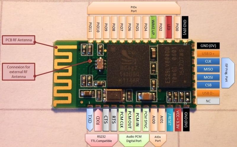
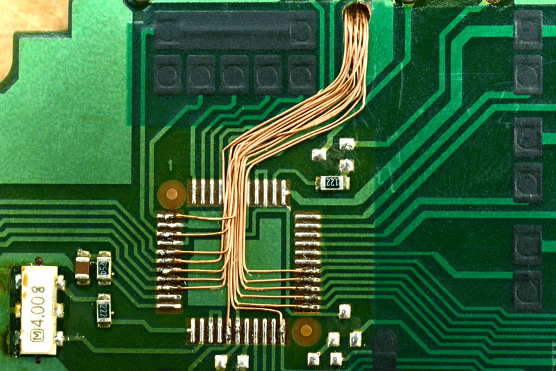
To see if it works we need to access the SPI pins on the HC-05. As you can see on this lovely pinout diagram, they're all grouped at the end.
It's at this point that most people build a special programming clip or holder, but I am far too lazy for that and just soldered some bits of wire straight to the board.
Again the wiring configuration is described on lorf's github page. I used 100ohm resistors as jumpers, it seemed like the right thing to do.
- DTR → CSB
- RTS → CLK
- RI → MOSI
- DSR → MISO
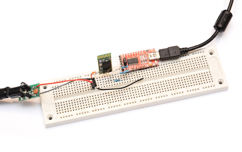
The device on the left is a bit of perfboard with a barrel jack and a 3.3V regulator on it. The FTDI board has a 3.3V output but it probably doesn't have the current capability for the HC-05, which can draw surprisingly high current at times (over 50mA).
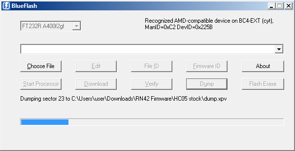
Open up BlueFlash, choose USB-SPI as the transport and see if you can connect to it. I can! Not just that, I can dump the stock firmware.
Brilliant. It's not just the flash that we have access to, there's also the Persistent Store, a separate bit of nonvolatile memory that has all the settings in it. These can be accessed using the PSTool.exe, which has a handy description for each one. The important one we want to watch out for is the Crystal Frequency Trim (PSKEY_ANA_FTRIM) located at 0x01F6 (choose view → sort by ordinal to find it).
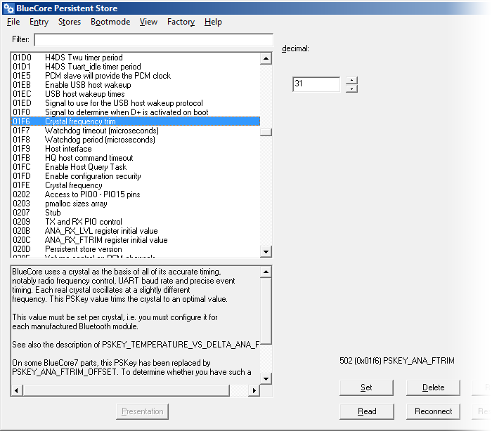
Write down what value this is, as we don't want to overwrite it. Another value to take note of is the bluetooth address (0x0001 PSKEY_BTADDR) which should be unique to each module. Byron's blog also recommends remembering the 0x01FE PSKEY_ANA_FREQ but this is just a divisor for the crystal frequency and should be the same as the RN-42.
It's probably good practice to dump the .psr of all the pskeys on the stock HC-05 too. In case you brick it, you know. Then again, it was only £2.
You are welcome at this point to buy a real RN-42, connect the SPI pins up and rip its firmware for porting to the HC-05, but this really goes against the spirit of piracy. I just googled for five minutes, a copy of the RN-42 firmware was not difficult to find. You'll need three files, the .xpv, .xdv and .psr.
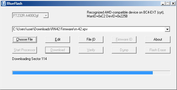
Select the XPV file (the XDV needs be in the same folder) in BlueFlash and hit download. This automatically does the erase first...
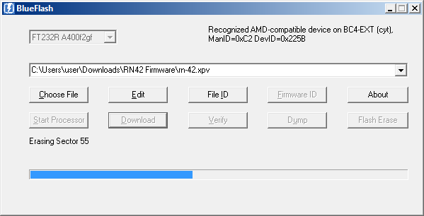
Then the downloading takes place.
Load up the PSTool again (note: close blueflash first, it tends to crash if they both try to access the chip at the same time) and select 'merge' to load your PSR file onto the chip. Finally, go through and change the crystal trim and bluetooth address back to their original values.
Congratulations, you now have an RN-42 module.
Building the HID joypad
Configuring the module
The RN-42 firmware supports Bluetooth HID: a wrapper for the USB HID (Human Interface Device) class. This is extremely attractive because it means a device can connect, tell the host it's a keyboard (or whatever), and start sending keypresses (or whatever) immediately, without needing extra software or drivers or anything. A gamepad is easy to do.I was somewhat surprised to learn that the RN-42 is even higher level than I was expecting. You can't directly set the HID report descriptors, only choose from a set bank of built-in ones. This doesn't really matter, only means we can't tell it exactly how many axes and buttons we have.
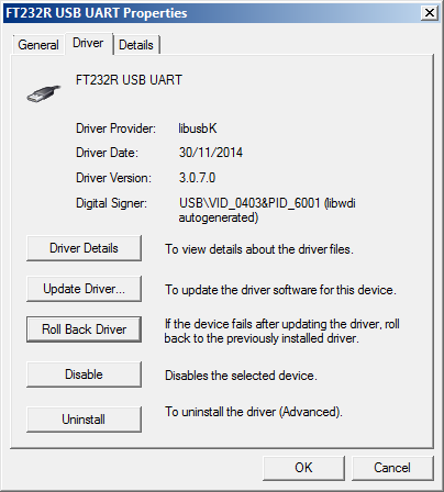
In order to configure and control the RN-42 née HC-05 we'd like to talk UART to it, and for that it'd be swell to have our old FTDI drivers back. This is as easy as opening up Device Manager, selecting the libusbK device and under properties clicking Roll Back Driver.
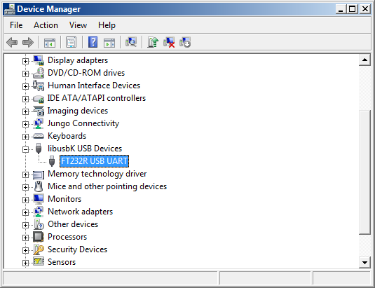
We have our COM ports again!
Tx and Rx are the first two pins. The default baud rate is 115200bps, 8N1.
Compared to the HC-05, the RN-42 uses a completely different but still fairly simple command set. Command mode is triggered by a sequence of three dollar symbols ($$$) followed by silence. It's important to wait a moment after this (i.e. make sure you don't send a CR or LF). You should be greeted by the response CMD.
The full command set is described in a lot of detail in the datasheet. All commands apart from the three dollar symbols need a CR line ending. Responses in grey, comments in green, here are the commands I used:
    $$$                    //Enter command mode (no CR/LF)
    CMD

    SM,6                   //Set Mode = pairing
    AOK

    SN,SNESpad             //Set Name
    AOK

    S~,6                   //Set profile = HID
    AOK

    SH,0240                //Set report descriptor = joypad
    AOK

    R,1                    //Reset for settings to take effect.
    Reboot!
This only has to be done once.
I turned on bluetooth on my laptop, found the device (SNESpad, yay) and paired to it. In order to send a report of the state of the buttons and axes, there's a fixed format that the RN-42 expects. The first byte needs to be 0xFD, to say that this is a raw report descriptor. The second byte is the length, which has to be six. The next six bytes describe the state of the controls, the last two being a bitwise mask of the buttons. I sent the following:
0xFD 0x06 0x00 0x00 0x00 0x00 0x55 0xAA
And saw this:
0x55 and 0xAA being my favourite bytes for generating a pretty pattern. Hooray! Next we need to grab a microcontroller and make it read the buttons and spit out the reports over UART.
But before we do that, let me ramble for a bit about which gamepad we're going to bluetoothify.
Choosing the gamepad
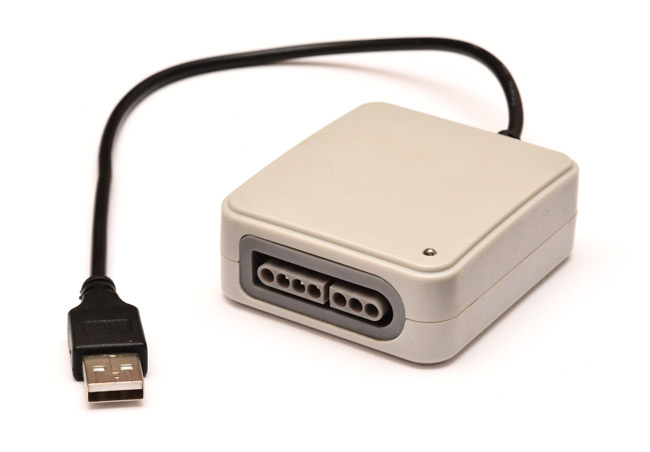
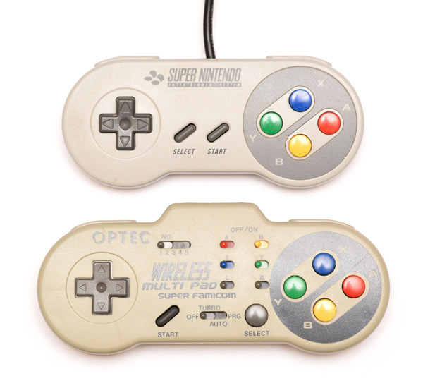
Ten years ago, having a real NES pad to use with your emulators made you the coolest kid on the block. Such was the demand for these things that China decided to cash in and you can now buy imitation NES pads with USB ports on the end. You can even get bluetooth ones. The Chinese pads tend to feel horrible and low quality, the buttons are all clicky in my experience. A far better device is a USB adapter, with the socket for an original controller. I have one and it's brilliant.
To be honest the best game controller is the PS3 sixaxis one. It's bluetooth, can function wired or wireless and works with your laptop emulators if you're willing to put the effort in. It's a fantastic controller, sort of the pinnacle of traditional game controllers, and apart from the rather horrible R2/L2 triggers and the fact you need to overwrite your original bluetooth drivers to get it to work, it's pretty much perfect.
So I don't really need a wireless NES pad. But I do have a couple of spare controllers to hand. (And by spare, I mean without any emotional attachment. I'd never tear up the controllers I actually used as a kid, of course.)
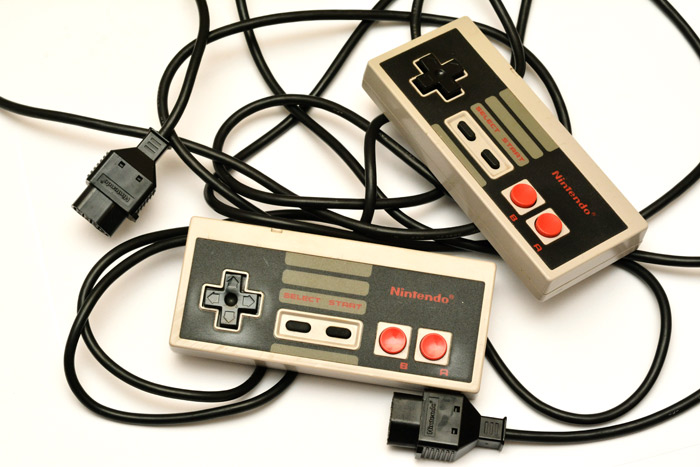
Yes, they look super cool. But I dislike the lack of buttons. With emulators it's become force of habit to press the fast forward button through all the boring bits, or maybe that's just a sign of my short attention span. Either way the lack of a FF button on the controller irritates me. I actually prefer to play NES games with a SNES pad for this reason.
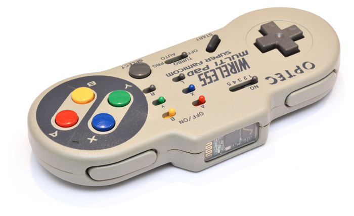
I didn't have a spare SNES pad though, so I hit up ebay for one. It has to be original, or it won't feel right. Then I saw something so ridiculous I had to buy it.
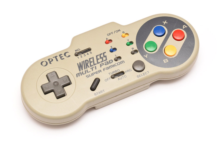
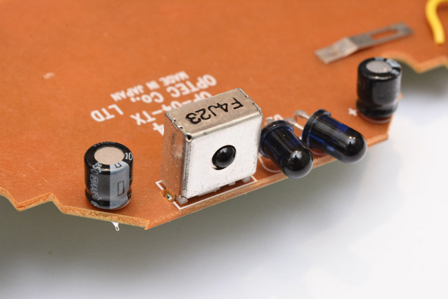
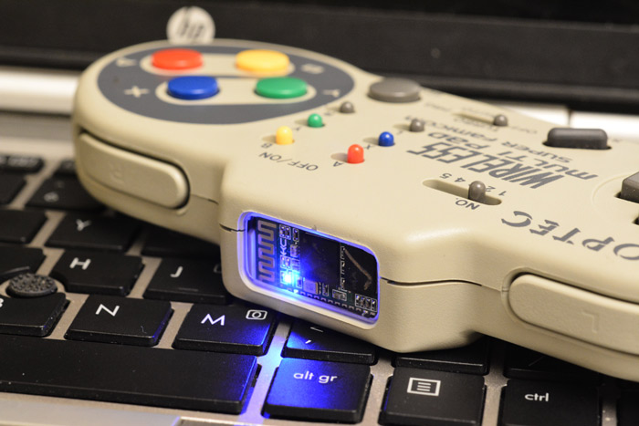
It's an infrared wireless SNES pad from 1994! Super Famicom indeed. Made in Japan. Optec—licensed by Nintendo. It's the kind of thing that actually goes for a lot of money if it's in the original box with all its bits. This one was missing the receive unit, which means it was cheap.
It is a little bit wider than the original controller. And the start/select buttons are the wrong way around. And I don't much care for the turbo functions. And the grey circle around the four buttons is painted on, not a sticker.
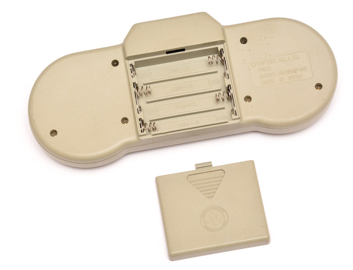
But the fact it says WIRELESS on it means, I think, we just have to do this. It also has a battery compartment for us. I was slightly looking forward to building a lithium battery charging circuit for this project (I've only done it once before and would like more practice) but using AAA batteries does actually make more sense. Realistically this is not going to see every day usage, and being able to pull the batteries out is a plus.
So it's decided. I hope there are people out there who adore this controller, and are about to scream as I ruin it permanently.
Building the gamepad
Opening it up, the first thing we notice is the battery pack is connected to the main board by springy metal tabs, not wires. This means the two parts come apart very easily. I approve of this construction technique.
I almost want to reverse engineer the IR protocol for this and build a new, IR base station that connects to USB. But for one, that wouldn't be bluetooth, and for two, the communication is actually bi-directional for some reason. This makes it much harder than just listening to what it sends as you press buttons. I think there must be some turn-on/go-to-sleep message it receives, since pressing the buttons did not seem to send anything.
I scoped the IR receiver as I pointed an ordinary remote at it (it happened to be a remote camera trigger) and it received it fine. The unit has Mitsumi written on it, and it seems to be doing the demodulation automatically, as it was giving a very clear digital signal out. Maybe I shall reuse this in a later project.
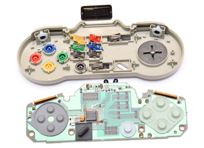
The membranes are all in excellent condition. And the whole thing is very clean. This evidently did not see much use.
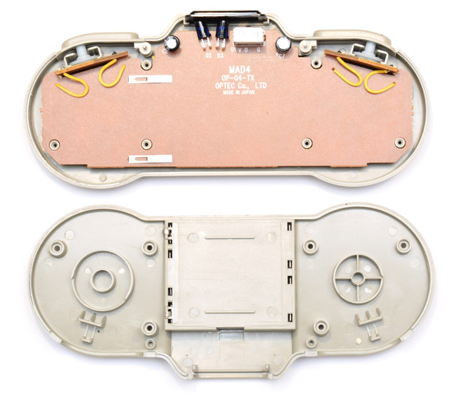
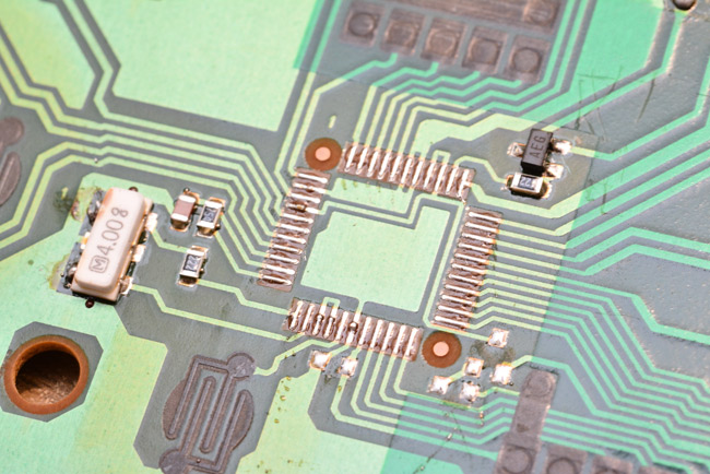
The chip is labelled NEC 65622 and the date code is 9442 = October 1994. This part is an ASIC gate array – yes, an FPGA without the FP bit. Must have been before epoxy blobs on PCBs became common. Gosh, the datasheet says it has 2,700 available gates!
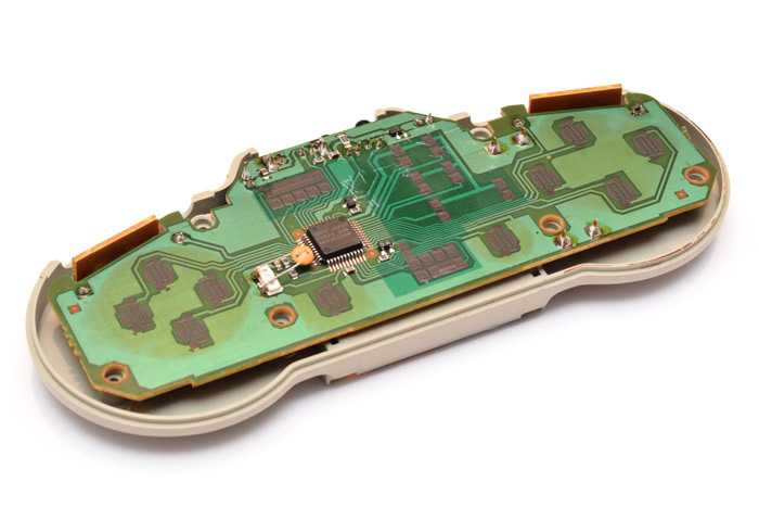
But it has to go. The only way to desolder a QFP-44 package is with a heat gun. It blew away some of the other parts around it too.
So the build begins. I think for now we'll ignore the turbo functions entirely, and just get the buttons / D pad working. I also plan to use the channel select switch as an on-off control. This means we have to solder fourteen wires to the 0.8mm pitch pads. We also have to route the wires very carefully, as the battery pack presses flat against the back of the circuit board, and the plastic mouldings around the switches and buttons press flat against the top of the board. I laugh in the face of such problems.
I think right angles definitely make your wires look more professional. Still not quite as tidy as ELM ChaN though.
With the IR parts removed, we now have all the wires we need coming out of the top, and a space available to put our new circuit in. Red and yellow are the battery terminals.
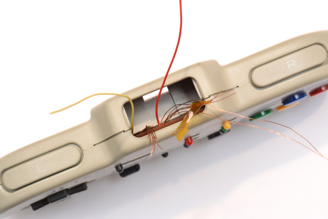
To have it screwed back together here is important. You can't actually test the buttons unless the case is shut. With the wires protruding through the very convenient IR window we're able to develop it without losing the ability to test it.
The first thing I measured was the resistance of the switch I'd chosen for on/off control, and as I suspected it was about 50 ohms, way too much for passing the full current through. We need to regulate the battery voltage down to 3.3V, but the regulators I had to hand weren't the type with an enable pin. The ideal thing to do here is build a high-side switch, cutting the power to the regulator, and the ideal part for doing that is a p-channel mosfet. I didn't have any of those either. But we can build an almost-as-good circuit with a PNP transistor.
Here's my hideous construction.
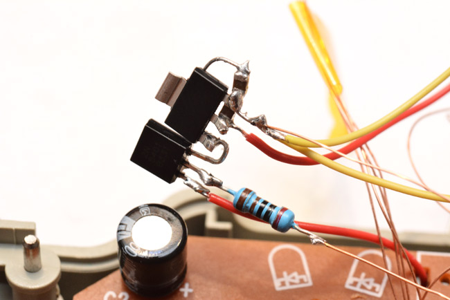
The wide part is an AMS1117-3.3 voltage regulator, with little surface mount 10uF ceramic caps to ground on the input and output legs. The PNP switches the battery voltage on when the base is switched, via the current-limiting resistor, to ground. In the 'off' state this circuit drew about 200nA, which isn't too bad.
Then all the other wires go the microchip. I chose an ATtiny2313 because it's super cheap, has enough pins and a UART port. The idea was to have the wires long enough that I could fit a test clip over the chip in order to program it, but short enough that we can squish it all into the space without having to shorten them afterwards.
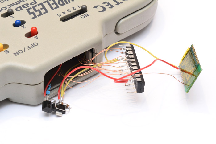
Something like this:
Time to program. Ha, we're basically building an asynchronous shift register. This did not take long to write.
.include "tn2313adef.inc"

    ldi r16, 1<<PD1      ; UART Tx
    out DDRD, r16
    ldi r16, 0
    out DDRB, r16
    ldi r16, $FF         ; Buttons
    out PORTB, r16
    ldi r16, 0b00111100  ; D-pad
    out PORTD, r16

    ldi r16, 8           ; UART 115200bps
    out UBRRL, r16
    ldi r16, 0
    out UBRRH, r16
    ldi r16, 1<<U2X
    out UCSRA, r16
    ldi r16, 1<<TXEN
    out UCSRB, r16

main:
    in r17, PINB
    com r17

    in r19, PIND
    andi r19, 0b00111100

    cp r20, r19          ; Only transmit if input state has changed
    cpc r18, r17
    breq main

    clr r21 ; X
    clr r22 ; Y

    sbrs r19, 2 ; Left
    subi r21, 127

    sbrs r19, 3 ; Up
    subi r22, 127

    sbrs r19, 4 ; Right
    subi r21, -127

    sbrs r19, 5 ; Down
    subi r22, -127

    ldi r16, $FD
    rcall sendByte
    ldi r16, $06
    rcall sendByte

    mov r16, r21
    rcall sendByte

    mov r16, r22
    rcall sendByte

    ldi r16, $00
    rcall sendByte

    ldi r16, $00
    rcall sendByte

    mov r16, r17
    rcall sendByte

    ldi r16, $00
    rcall sendByte


    mov r18, r17         ; Store input states of last transmit
    mov r20, r19

rjmp main


sendByte:
    sbis UCSRA,UDRE
    rjmp sendByte
    out UDR, r16
    ret
After testing it worked (which unsurprisingly, it did) I then shoved it all into the recess. Actually it wasn't that tight a fit at all.
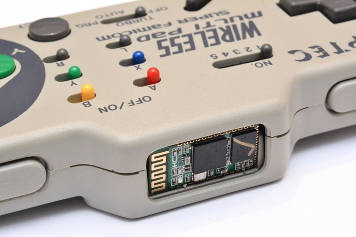
It actually looks pretty cool, and seems a shame to hide it behind the infrared window. So I decided to craft a new window out of clear acrylic, using a combination of the laser cutter and a file. I couldn't think of a clever way of doing it, so just etched a guide as to where it needed to be filed by hand.
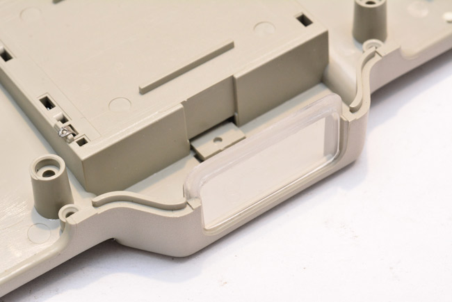
Seems to fit.
Did I mention there's a blue LED on the HC-05 module?
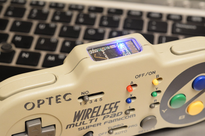
It's actually pretty dim – which is good for battery life – but through the magic of long exposures we can make it SHINE.
Excellenté.
Now if you'll excuse me, I'm off to play some Mario.