
Etching PCBs with a Laser Cutter
24 Apr 2016Progress: Complete
Much as I enjoy creative point-to-point wiring, there are times when one really does need a PCB.
I had an idea for using the laser cutter to produce PCBs. The idea is to reduce the number of steps involved in the process, if possible. There are a bazillion guides out there for making PCBs at home, most of them involve multiple steps and different chemicals and seem like more effort than it's worth. Just about the only single-step production method is routing the board – unfortunately I don't have a CNC router. Yet.
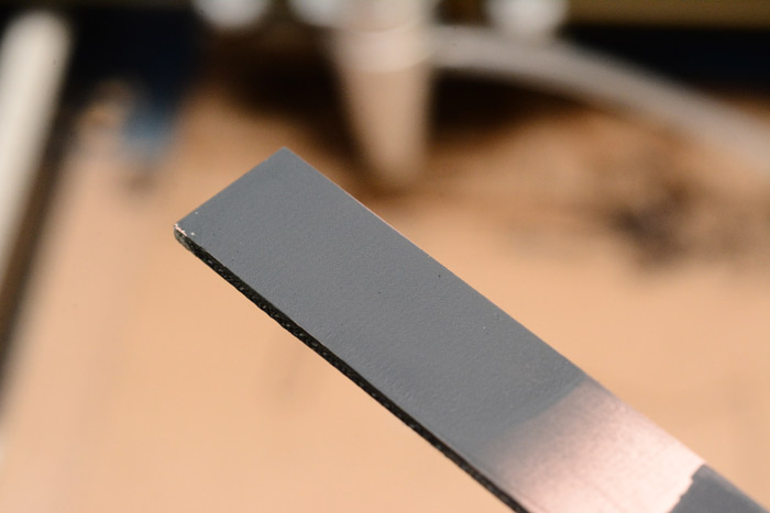
My laser is one of the dirt-cheap 40W ones from ebay, and there's no way it can etch copper directly, it just wicks the heat away instantaneously. My idea was to spray-paint the copper-clad board, etch away the paint, then dip the board in the copper-dissolving acid (Ferric Chloride). This should hopefully be easier and quicker than the ordinary photoresist method, and more accurate and repeatable than the toner-transfer method.
I started by buying some really cheap copper-clad FR4 board. I cut off a strip, and sprayed it with ordinary black spray paint. Then etched some test patterns.
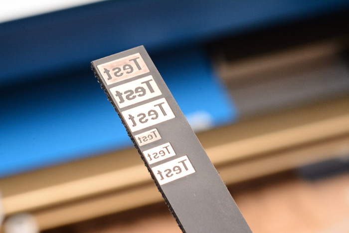
Heh, this is also a helpful reminder than Moshidraw's etching mirrored/not-mirrored options are mislabelled. Each one was done at a different setting. Power doesn't seem to make much difference, but the number of passes does. The first one is a single pass and there's a visible residue of paint left behind. I think this is due to the pathetic flow from my air assist, and the paint-vapour is re-settling. Doing multiple passes removes the residue.
I then dabbed a small amount of ferric chloride onto the board with a sponge. This took maybe twenty minutes to etch through the copper. I periodically agitated it with the sponge. It probably would have been quicker if I were less conservative with the acid. The third pattern was the first to finish etching, and I stopped it just after for fear of over-etching, but amazingly all of the tests worked really well.
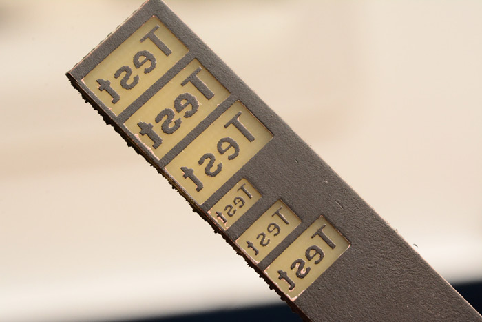
We can then wipe the paint away with IPA. By the way, the third pattern has the thinnest lines because I did three passes and I think I slightly jigged the table between them, the board was not held down.
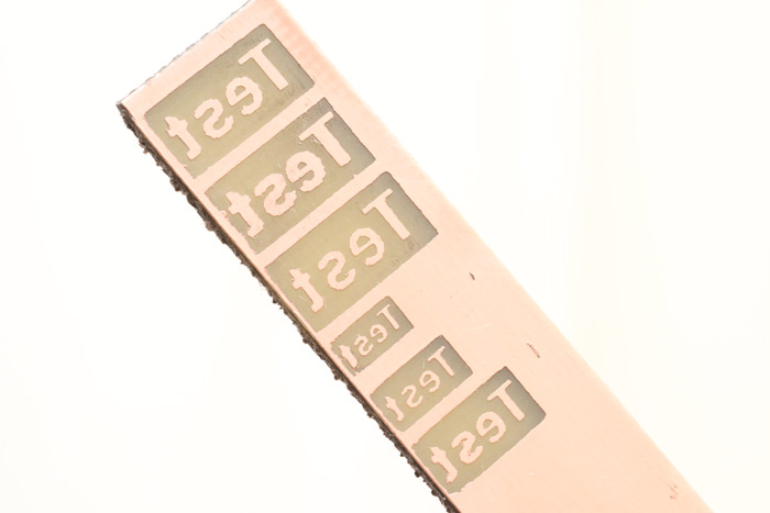
To be honest I was probably over-thinking the whole thing, and it seems that pretty much any laser settings will work for this. Brilliant.
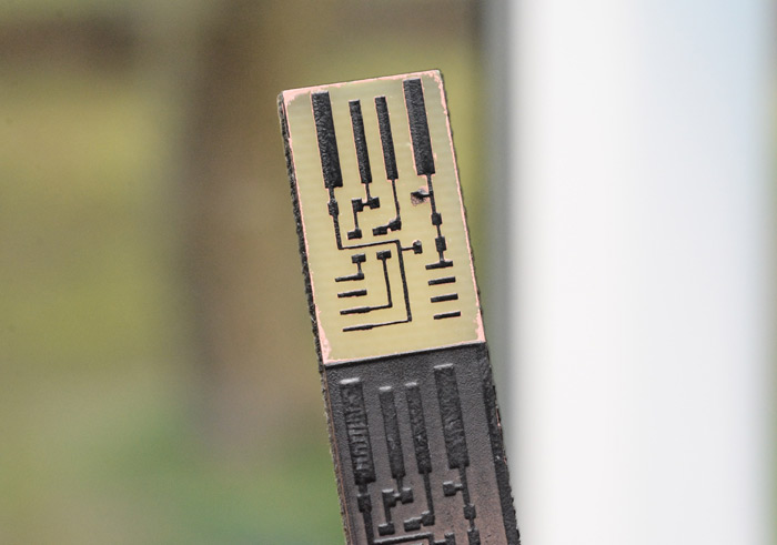
Let's do an actual PCB. Although I do have an actual project in mind – that's the reason we're doing this – I think something simple would be a good start. Let's make a generic ATtiny85 USB circuit. Ha harr, this is the modern-day equivalent of a 555 timer circuit.
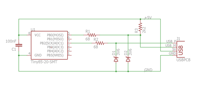
Since it's a PCB I thought I'd make use of the USB PCB edge-connector type thingamabob. Sparkfun's eagle library has one of these already made up, that's cool. My only complaint is that they stuck the pins on the schematic symbol in an apparently random order. Err, why not just have them match the actual pads? Eh.
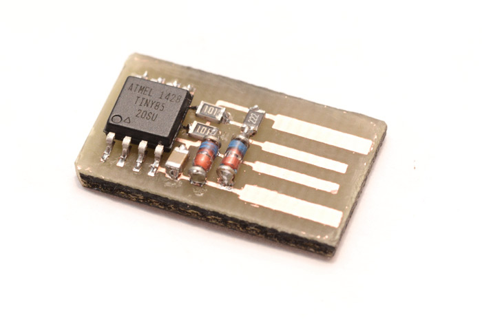
When it comes to laying out PCBs I am a stickler for extremely cramped designs. More efficient usage of space! Also, doing it all on the top layer and using surface mount parts means no drilling required.
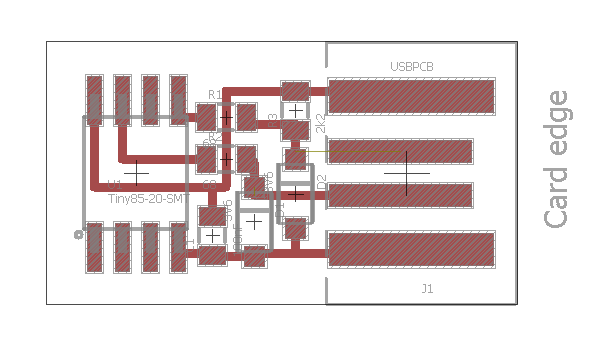
I managed to arrange it that all of the pins of the ATtiny85 are exposed outwards. This should be very useful if or when we reuse this design for more complex USB devices. Also it looks neater.
Next we export this design as an image at 254 DPI. I like this resolution since it's exactly 10 pixels per millimetre, and moshidraw is all about millimetres. Here's the actual image I'm etching.
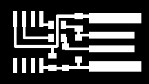
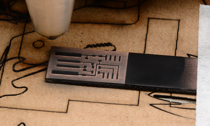
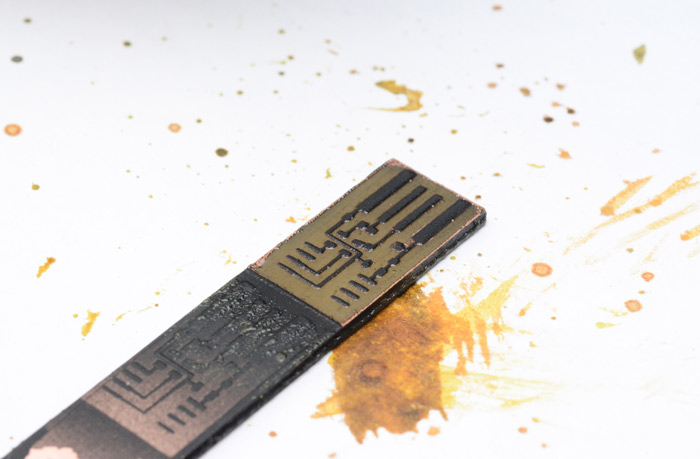
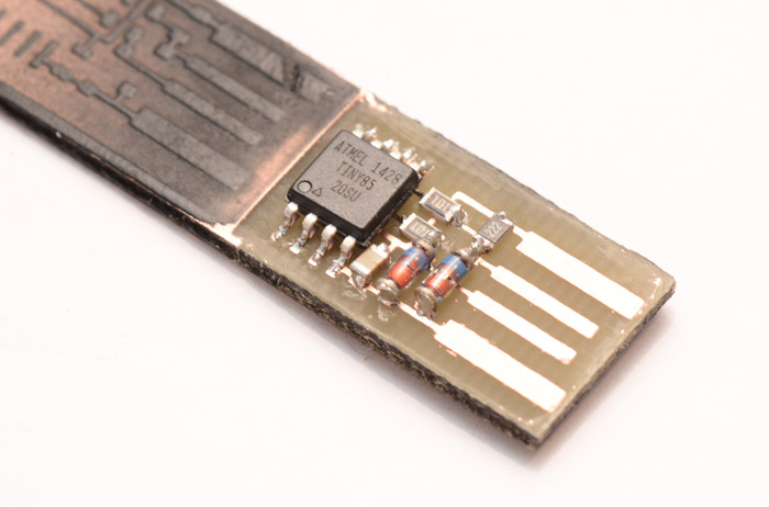
The test strip above turned out to be just wide enough for my new circuit, so I wiped off the back and sprayed a new layer of paint.
This time I taped it down. To line it up, I did an extremely weak etch onto the cardboard underneath and visually placed the board on top.
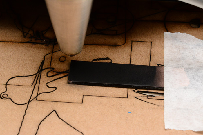
Yep, that's the outline of a guitar keyring I made for a friend the other day.
First pass...
And a second pass to remove the residue.
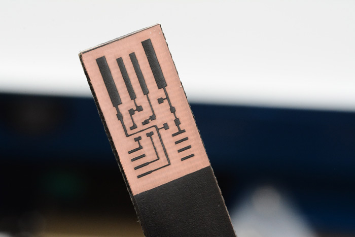
I think the laser was slightly out of focus. I don't have a Z-axis, I just set the focus by stacking bits of cardboard underneath the work. The traces are a bit too thin as a result. Since it only takes a minute to make this, I (kinda pointlessly) decided to re-spray and re-etch to see if we could do better.
So I etched a few times at different heights, maybe I slightly improved it, but I didn't realize I'd actually been really lucky with the alignment the first time. The next two attempts weren't nearly as well centred as the first. This problem could be completely avoided by using a bigger piece of copper-clad board and cutting it to size afterwards. Or using a positioning system more advanced than cardboard and masking tape.
I felt like I was wasting time, so I decided to just go with this one, even though it's worse than the first attempt.
It's difficult to take pictures while you're working with the chemicals. Or chemical. This is the amount of ferric chloride I used, dabbed on with a sponge. I'm using just a plain piece of paper to catch the drips, it doesn't seem to dissolve through it.
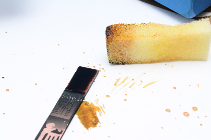
The advantage of this method is that all of the dissolved copper ends up as a green stain on a piece of kitchen towel, instead of back in the bottle. I then just binned the kitchen towel, I'm not sure how good for the environment this is, but it's certainly better than it going down the drain, and the bottled ferric chloride I'm left with is still at full strength.
Every minute or so I wipe the acid around to see how it's doing. Annoyingly you get no feedback on how far it has to go until it's already there.
Not bad, not bad at all.
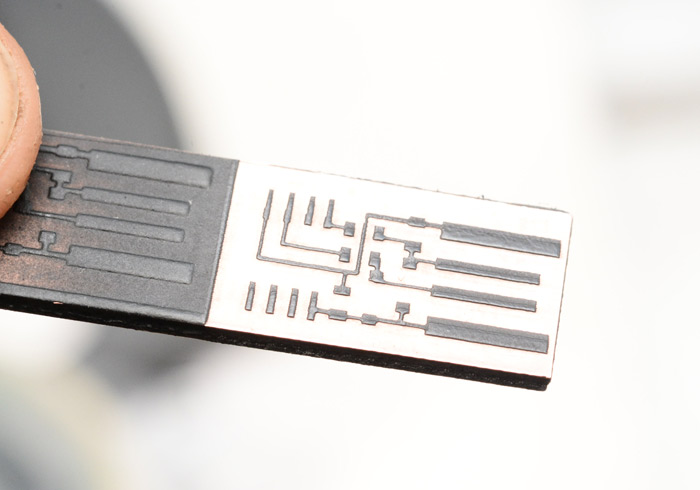
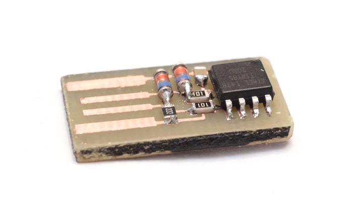
Wipe off the paint with IPA. The edges of the board still had some copper to them, I scraped these off with the edge of a ruler.
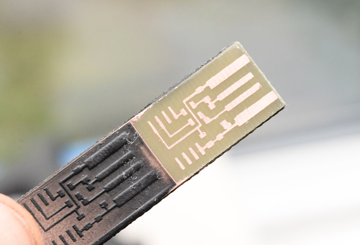
The traces certainly are thin, but the only way to tell if they're too thin, is to assemble and solder.
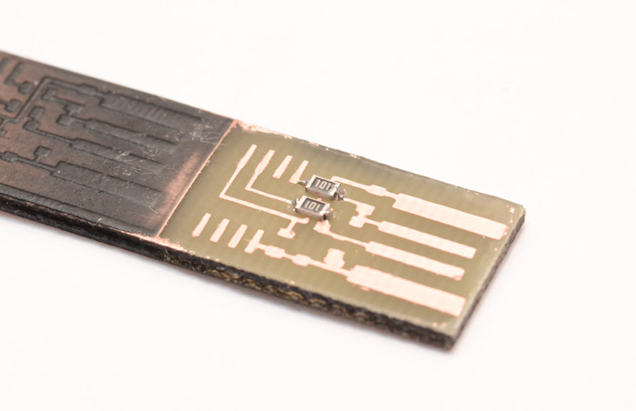
Tweezers certainly are useful.
Now for the moment of truth, as I jam the thing into a USB port. It works!
Now we can chop the excess board away.
I filed one side to make it fit into the USB port more easily.
Of course I haven't actually decided what to do with this yet, but that's not a problem, because reprogramming it is easy:
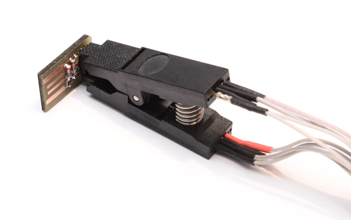
That's what you call In-System Programming if I've ever seen it. Those test clips are about £4 and worth every penny.
I think I might turn this into a usb keyboard that hits capslock every ten minutes or so. I've been meaning to make one of those.
As for etching a PCB with a laser, I think we can call it a success. Of course, for a "professional" result we would need a green solder resist. This isn't even that expensive, but since this is currently such a quick process (spray paint / laser / acid) I don't know if I want to add it. The normal method is UV cure, which means you need a mask for it, and since I'm not doing the photoresist this isn't convenient at all. I think we need a type of solder-resist that sprays on, and then we ablate it with the laser where we don't want it.
But overall the process I've shown on this page is much easier than, for instance, developing film. Hooray!